Glue sealing system and method for optical fiber sensing probe
An optical fiber sensing probe and optical fiber technology, which is used in thermometer parts, thermometers with physical/chemical changes, measuring devices, etc., can solve the problems of low reliability of sealing products, easy deviation of bonding positions, and batch processing efficiency Low problems, to achieve the effect of improving curing efficiency, high packaging yield, and convenient connection and separation
- Summary
- Abstract
- Description
- Claims
- Application Information
AI Technical Summary
Problems solved by technology
Method used
Image
Examples
Embodiment 1
[0058] The present invention analyzes the two traditional encapsulation methods, both of which belong to a single thermal curing encapsulation. The thermal curing method itself has the disadvantages of multiple curing stages and long time, but it has strong adhesive force, high curing firmness, and outstanding high temperature resistance. In contrast, the light curing method has the advantage of fast curing speed, but the traditional light curing adhesive is usually cured by UV glue, which is fast but has low temperature resistance. Therefore, the present invention adopts UV hybrid system glue, which can be pre-cured by light before use, and then heat-cured after tens of seconds of curing, so that it can achieve stronger curing performance and temperature resistance.
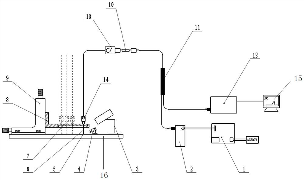
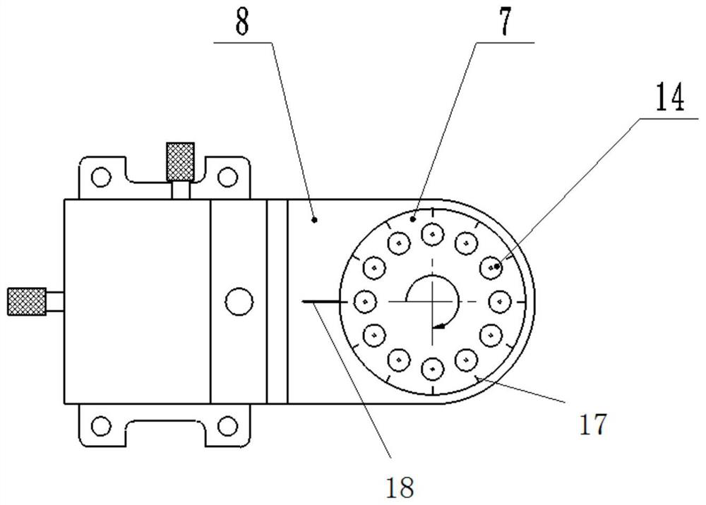
[0059] Such as figure 1 As shown, a kind of sealing system for optical fiber sensing probe, the optical fiber sensing probe is a sealed part, which includes a semiconductor chip 5 and an optical fiber 6 positio...
Embodiment 2
[0083]The difference from Embodiment 1 is that the working process of the glue sealing system:
[0084] 1) Clamp an optical fiber 6 to be bonded on one of the lower end optical fiber holders 14, and the lower end of the optical fiber 6 passes through the through hole of the rotary tooling 7 and is located above the installation platform 16;
[0085] 2) Rotate the rotary tooling 7 so that the optical fiber 6 in step 1) is located within the illumination range of the curing light source 4, the upper end of the optical fiber 6 is installed on the upper end optical fiber holder 13, and a semiconductor wafer 5 is placed on the installation platform 16 , the semiconductor wafer 5 is located below the optical fiber 6;
[0086] 3) Turn on the light source driving circuit 1, the light source driving circuit 1 drives the light source of the light source module 2 to emit light, the initial optical signal passes through the optical fiber coupler 11 and the optical fiber connector 10, reac...
PUM
 Abstract
Description
Claims
Application Information

