Preparation method of vertical-gate semiconductor device

A semiconductor and vertical gate technology, applied in the field of vertical gate semiconductor device preparation, can solve the problem of uneven electrical performance of image sensors

Pending Publication Date: 2021-04-06
SHANGHAI HUALI MICROELECTRONICS CORP
View PDF4 Cites 1 Cited by
  • Summary
  • Abstract
  • Description
  • Claims
  • Application Information

AI Technical Summary

Problems solved by technology

[0004] The purpose of the present invention is to provide a method for preparing a vertical g...

Method used


Image

  • Preparation method of vertical-gate semiconductor device
  • Preparation method of vertical-gate semiconductor device
  • Preparation method of vertical-gate semiconductor device

Examples


preparation example Construction

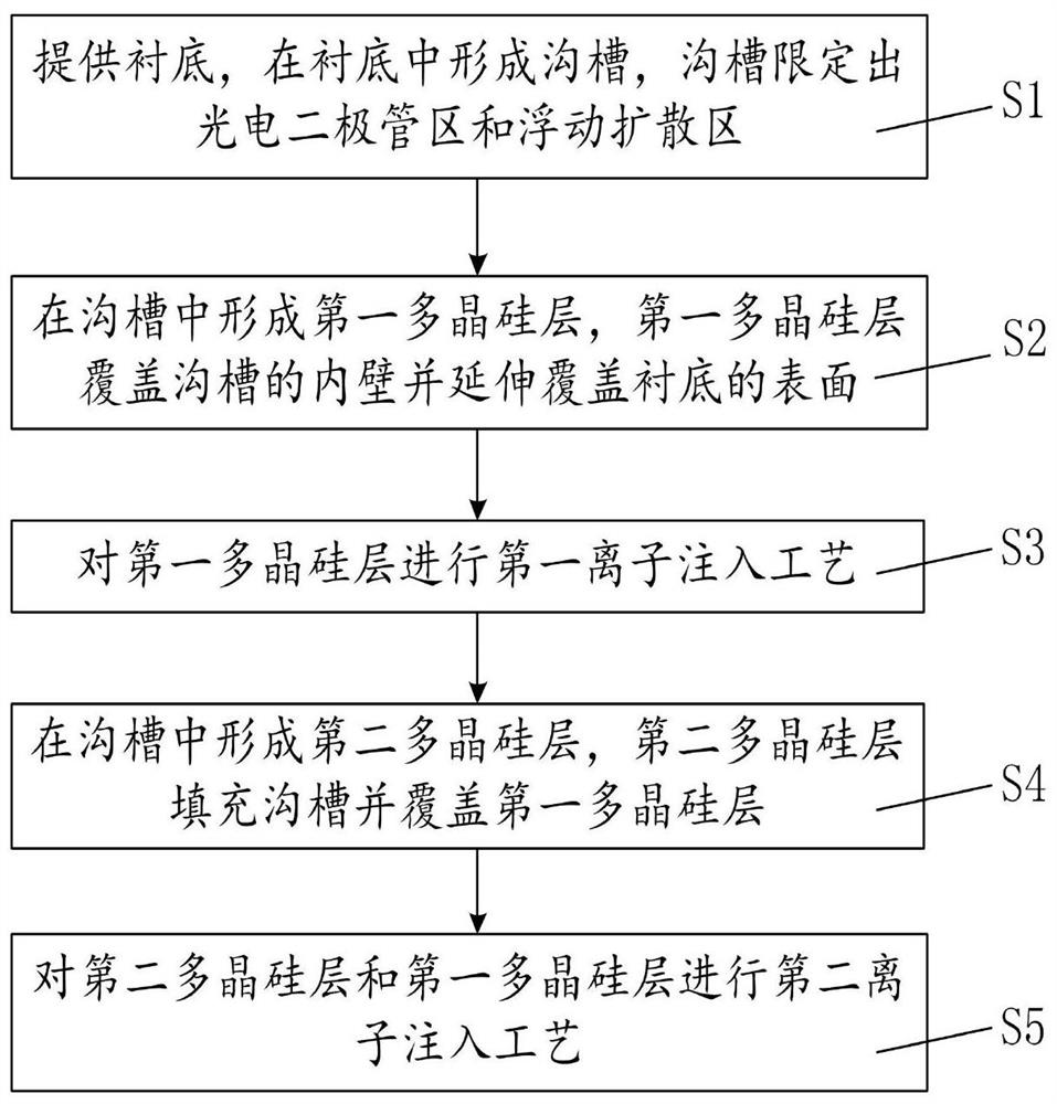
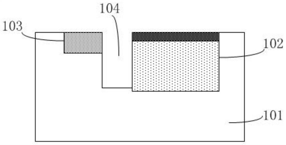
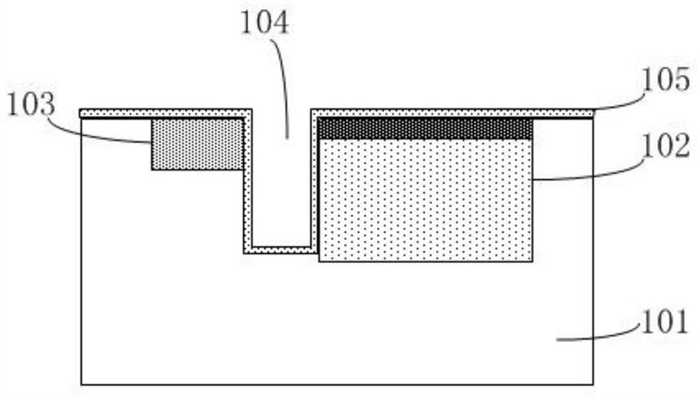
[0026] figure 1 A flowchart of a method for manufacturing a vertical gate semiconductor device provided in this embodiment, Figure 2A-2D A schematic structural diagram of a method for fabricating a vertical gate semiconductor device provided in this embodiment. This embodiment provides a method for fabricating a vertical gate semiconductor device, which is used to improve the phenomenon of uneven electrical properties of image sensors. Please refer to figure 1 ,include:

[0027] Step S1: providing a substrate, forming a trench in the substrate, the trench defines a photodiode region and a floating diffusion region;

[0028] Step S2: forming a first polysilicon layer in the trench, the first polysilicon layer covers the inner wall of the trench and extends to cover the surface of the substrate;

[0029] Step S3: performing a first ion implantation process on the first polysilicon layer;

[0030] Step S4: forming a second polysilicon layer in the trench, the second polysili...


PUM


Abstract

The invention provides a preparation method of a vertical-gate semiconductor device. The preparation method comprises the following steps: providing a substrate; forming a trench in the substrate, wherein the trench defines a photodiode region and a floating diffusion region; forming a first polycrystalline silicon layer in the trench, wherein the first polycrystalline silicon layer covers the inner wall of the trench and extends to cover the surface of the substrate; performing a first ion implantation process on the first polycrystalline silicon layer; forming a second polycrystalline silicon layer in the trench, wherein the trench is filled with the second polycrystalline silicon layer, and the second polycrystalline silicon layer covers the first polycrystalline silicon layer; and performing a second ion implantation process on the second polycrystalline silicon layer and the first polycrystalline silicon layer. According to the invention, the phenomenon of non-uniform electrical performance of an image sensor is improved.

Description

technical field [0001] The invention relates to the technical field of semiconductors, in particular to a method for preparing a vertical gate semiconductor device. Background technique [0002] A traditional image sensor consists of a photodiode and a transistor. During the working process of the image sensor, the photodiode needs to transfer photoelectrons to the floating diffusion region, and then convert the charge into a voltage for amplification and output. For the 2D planar gate structure, when the transfer gate of the transfer transistor is turned on, the photoelectrons in the photodiode region are transmitted to the floating diffusion region through the surface channel of the planar gate, and then read. This transmission method has a small path, which is not conducive to fast reading It will also lead to low efficiency of the image sensor. [0003] The 3D vertical gate structure solves the problem of slow photoelectron transfer and low efficiency. The 3D vertical g...

Claims


Application Information

Patent Timeline
IPC IPC(8): H01L27/146
CPCH01L27/14614H01L27/14689H01L27/14687
Inventor 陈彩云张磊顾珍董立群王奇伟陈昊瑜
Owner SHANGHAI HUALI MICROELECTRONICS CORP
Why Eureka
Try Eureka