Method for improving doping uniformity of semiconductor laser

A laser and semiconductor technology, applied to the structure of the active region, gaseous chemical plating, metal material coating process, etc., can solve the problem that the uniformity of doping concentration cannot meet the required requirements, and achieve the promotion of mass production, Effect of improving doping uniformity and reducing the influence of doping unevenness

Active Publication Date: 2021-04-16
SUZHOU EVERBRIGHT PHOTONICS CO LTD +1
View PDF5 Cites 1 Cited by
  • Summary
  • Abstract
  • Description
  • Claims
  • Application Information

AI Technical Summary

Problems solved by technology

[0004] In view of this, an embodiment of the present invention provides a method for improving the doping uniformity of a semiconductor laser to solve the technical problem in the prior art that the doping concentration uniformity of the doping source on the epitaxial layer cannot meet the required requirements

Method used


Image

  • Method for improving doping uniformity of semiconductor laser
  • Method for improving doping uniformity of semiconductor laser
  • Method for improving doping uniformity of semiconductor laser

Examples


Embodiment 1

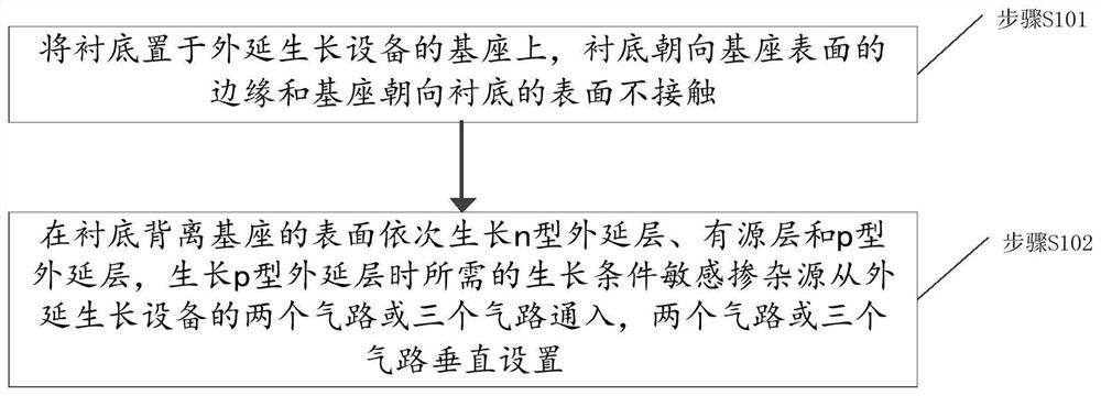
[0032] An embodiment of the present invention provides a method for improving the doping uniformity of a semiconductor laser, such as figure 1 As shown, the method includes the following steps:

[0033] Step S101: The substrate is placed on the base of the epitaxial growth equipment, and the edge of the substrate facing the surface of the base is not in contact with the surface of the base facing the substrate; in a specific embodiment, the epitaxial growth equipment can be made of metal Organic compound chemical vapor deposition (Metal-organic Chemical Vapor Deposition, MOCVD) equipment.

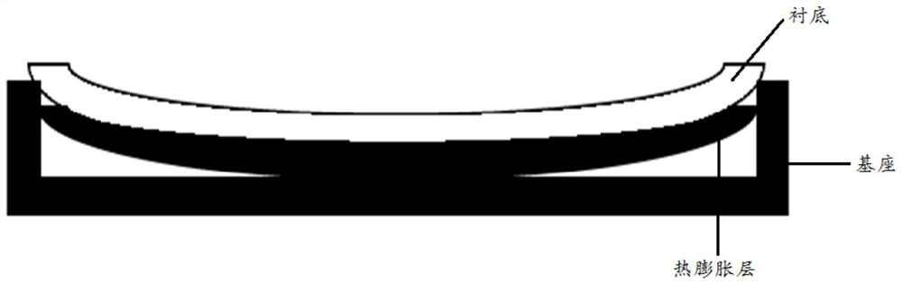
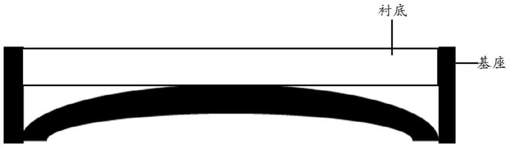
[0034] In order to keep the edge of the substrate out of contact with the base, in one embodiment, before placing the substrate on the base, a thermal expansion layer can be deposited on one side of the substrate, and the thermal expansion coefficient of the thermal expansion layer is greater than that of the substrate. When the substrate is placed on the base of the epitaxial growth equip...

Embodiment 2

[0043] The method for improving the doping uniformity of a semiconductor laser provided by an embodiment of the present invention is described by taking an edge-emitting semiconductor laser as an example, wherein the edge-emitting semiconductor laser is a 980 nm edge-emitting semiconductor laser.

[0044] First, adjust the temperature uniformity of the substrate surface during epitaxial growth. Specifically, silicon nitride can be deposited on the back of the gallium arsenide substrate by using PECVD or LPCVD process. The thickness of the deposited silicon nitride is 100nm-2000nm. By adjusting the substrate parameters of silicon nitride, the thermal expansion coefficient of silicon nitride can be made greater than the thermal expansion coefficient of the gallium arsenide substrate, when the gallium arsenide substrate is placed on the base of the MOCVD equipment for heating, the silicon nitride film will produce compressive strain, and the gallium arsenide substrate will become ...

Embodiment 3

[0049] The method for improving the doping uniformity of a semiconductor laser provided by the embodiment of the present invention is described by taking a vertical cavity surface emitting semiconductor laser as an example, wherein the vertical cavity surface emitting semiconductor laser is a 940nm vertical cavity surface emitting semiconductor laser.

[0050] First, adjust the temperature uniformity of the substrate surface during epitaxial growth. Specifically, silicon nitride can be deposited on the back of the gallium arsenide substrate by using PECVD or LPCVD process. The thickness of the deposited silicon nitride is 100nm-2000nm. By adjusting the substrate parameters of silicon nitride, the thermal expansion coefficient of silicon nitride can be made The thermal expansion coefficient of the gallium arsenide substrate is greater than that of the gallium arsenide substrate. When the gallium arsenide substrate is placed on the base of the MOCVD equipment for heating, the sil...


PUM

PropertyMeasurementUnit
thicknessaaaaaaaaaa
thicknessaaaaaaaaaa
thicknessaaaaaaaaaa

Abstract

The invention discloses a method for improving the doping uniformity of a semiconductor laser, and the method comprises the steps: placing a substrate on a pedestal of epitaxial growth equipment, and enabling the edge, facing the surface of the pedestal, of the substrate not to be in contact with the surface, facing the substrate, of the pedestal; sequentially growing an n-type epitaxial layer, an active layer and a p-type epitaxial layer on the surface, deviating from a base, of a substrate, introducing a growth condition sensitive doping source required for growing the p-type epitaxial layer from two or three gas paths of epitaxial growth equipment, and vertically arranging the two or three gas paths. By implementing the invention, the contact between the substrate and the base is changed, so that the contact between the edge of the substrate and the edge of the base becomes poor, the temperature uniformity of the surface of the substrate can be effectively adjusted, and the influence of the temperature on the non-uniform doping of the doping source can be reduced; moreover, two or three paths of doping sources sensitive to the growth condition are simultaneously introduced, so that the doping uniformity of the doping sources sensitive to the growth condition can be improved on the basis of reducing the influence of the temperature on the doping uniformity of the doping sources sensitive to the growth condition.

Description

technical field [0001] The invention relates to the technical field of semiconductors, in particular to a method for improving the doping uniformity of semiconductor lasers. Background technique [0002] Semiconductor laser is an important optoelectronic device, which has a wide range of applications in sensing, lighting, communication, pumping and other fields. In order to reduce the manufacturing cost of semiconductor lasers, three-inch, four-inch and even six-inch gallium arsenide substrates are gradually used in the epitaxy process. At present, planetary reaction chambers are often used to grow epitaxial wafers for semiconductor lasers, and a combination of substrate rotation and graphite disk revolution is used to achieve uniform growth of epitaxial layers on the entire substrate surface. By adopting the above solution, the standard deviation of the thickness of the epitaxial layer over the entire epitaxial layer can be less than 0.5%. [0003] However, when the epita...

Claims


Application Information

Patent Timeline
Patent Type & Authority Applications(China)
IPC IPC(8): H01S5/30C23C16/30C23C16/34C23C16/50C23C16/52
CPCY02P70/50
Inventor 程洋郭银涛王俊刘恒
Owner SUZHOU EVERBRIGHT PHOTONICS CO LTD
Why Eureka
Try Eureka