

Method for enhancing ohmic contact of gallium oxide semiconductor device
A technology of ohmic contact and gallium oxide, which is applied in semiconductor devices, semiconductor/solid-state device manufacturing, electrical components, etc., can solve the problems of difficult control of ohmic contact depth, great influence of ohmic contact annealing time and temperature, high annealing temperature, etc. , to achieve the effect of good flatness, low annealing temperature and low roughness
- Summary
- Abstract
- Description
- Claims
- Application Information
AI Technical Summary
Problems solved by technology
Method used
Image

Examples
Embodiment 1
[0050] A method for enhancing the ohmic contact of a gallium oxide semiconductor device, comprising the following steps:
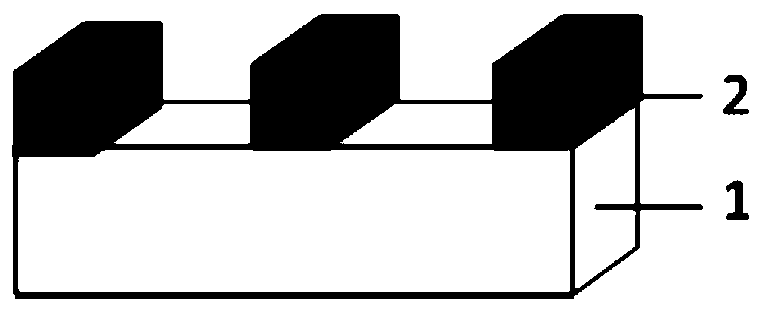
[0051] (1) Use a photolithography process to define a pattern that needs to enhance the ohmic contact area on the upper surface of the gallium oxide substrate 1, expose the defined area on the upper surface of the gallium oxide substrate 1, and cover the remaining area with a photoresist to form ions Implanted with photoresist layer 2, as figure 1 shown;
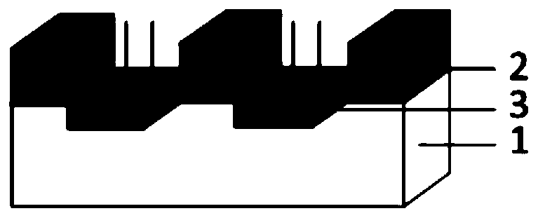
[0052] (2) Implant silicon dopant ions on the upper surface of the gallium oxide substrate 1 with a doping concentration of 2.5×10 15 cm -3, the process of doping ions adopts an ion implantation process to form an ion implantation layer 3, such as figure 2 shown;
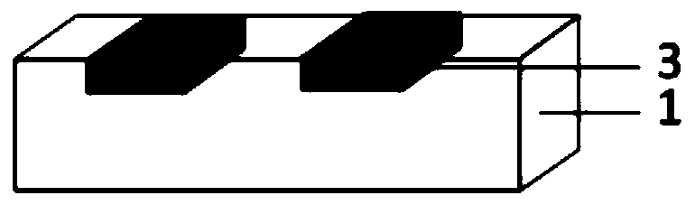
[0053] (3) After the ion implantation is completed, remove the photoresist on the upper surface of the gallium oxide substrate, such as image 3 shown;
[0054] (4) Perform heat treatment on the gallium oxide substrate that has been ion...
Embodiment 2
[0060] A method for enhancing the ohmic contact of a gallium oxide semiconductor device, comprising the following steps:
[0061] (1) Use a photolithography process to define a pattern that needs to enhance the ohmic contact area on the upper surface of the gallium oxide substrate 1, expose the defined area on the upper surface of the gallium oxide substrate 1, and cover the remaining area with a photoresist to form ions Implanted with photoresist layer 2, as figure 1 shown;
[0062] (2) Implanting platinum dopant ions on the upper surface of the gallium oxide substrate 1 with a doping concentration of 1×10 15 cm -3 , the process of doping ions adopts an ion implantation process to form an ion implantation layer 3, such as figure 2 shown;
[0063] (3) After the ion implantation is completed, remove the photoresist on the upper surface of the gallium oxide substrate, such as image 3 shown;
[0064] (4) Perform heat treatment on the gallium oxide substrate that has been ...
Embodiment 3
[0070] A method for enhancing the ohmic contact of a gallium oxide semiconductor device, comprising the following steps:
[0071] (1) Use a photolithography process to define a pattern that needs to enhance the ohmic contact area on the upper surface of the gallium oxide substrate 1, expose the defined area on the upper surface of the gallium oxide substrate 1, and cover the remaining area with a photoresist to form ions Implanted with photoresist layer 2, as figure 1 shown;
[0072] (2) Zinc doping ions are implanted on the upper surface of the gallium oxide substrate 1 with a doping concentration of 5×10 16 cm -3 , the process of doping ions adopts an ion implantation process to form an ion implantation layer 3, such as figure 2 shown;
[0073] (3) After the ion implantation is completed, remove the photoresist on the upper surface of the gallium oxide substrate, such as image 3 shown;
[0074] (4) Perform heat treatment on the gallium oxide substrate that has been i...
PUM
| Property | Measurement | Unit |
|---|---|---|
| Thickness | aaaaa | aaaaa |
| Thickness | aaaaa | aaaaa |
| Thickness | aaaaa | aaaaa |
Abstract
Description
Claims
Application Information