Method for improving silicon wafer bonding force

A technology of bonding force and silicon wafers, which is applied in the manufacture of electrical components, circuits, semiconductors/solid-state devices, etc., can solve the problems of high surface roughness and integrity of silicon wafers, expand the scope of silicon wafers, solve limitations, Guarantee the effect of yield and quality

Pending Publication Date: 2021-04-16
长春长光圆辰微电子技术有限公司
View PDF6 Cites 0 Cited by
  • Summary
  • Abstract
  • Description
  • Claims
  • Application Information

AI Technical Summary

Problems solved by technology

In order to improve the bonding strength, it is sometimes necessary to pressurize and bond under a certain vacuum condition, but this metho

Method used


Image

  • Method for improving silicon wafer bonding force
  • Method for improving silicon wafer bonding force
  • Method for improving silicon wafer bonding force

Examples


Embodiment

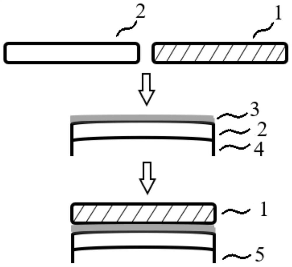
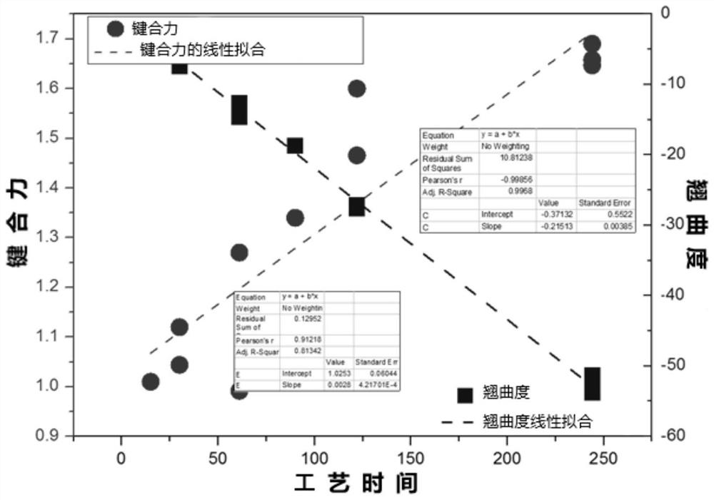
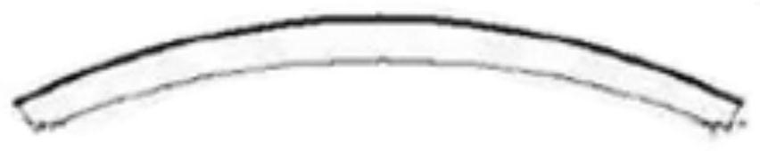
[0030] The present invention provides a method for improving the bonding force of silicon wafers. A silicon dioxide film 3 is grown on one of the silicon wafers using a plasma chemical vapor deposition process, so that the warpage (bow value) of the silicon wafers is about -50 μm, and then the The two silicon wafers are bonded and annealed at normal temperature and pressure, thereby improving the bonding force of the silicon wafers.

[0031] Such as figure 1 It is an experimental flow chart of a method for improving the bonding force of silicon wafers of the present invention.

[0032] Such as figure 1 Shown, the specific operation steps of the present invention are:

[0033] S1: Prepare two silicon wafers; and set one as the upper silicon wafer 1 to be bonded, and the other as the lower silicon wafer 2 to be bonded.

[0034] S2: Select the lower silicon wafer 2 to perform a film deposition process, and grow a silicon dioxide film 3 on the surface;

[0035] S3: Bonding two...


PUM


Abstract

The invention provides a method for improving silicon wafer bonding force, and is characterized in that a silicon dioxide film grows on one silicon wafer through plasma chemical vapor deposition; and two silicon wafers are bonded and annealed at normal temperature and normal pressure. According to the invention, the problem of low bonding strength of two silicon wafers at normal temperature and normal pressure is solved, the use limitation of the silicon wafers is improved, the available silicon wafer range is expanded, the bonding strength of the bonded silicon wafers is improved, and the yield and quality of products are ensured.

Description

technical field [0001] The invention relates to the field of semiconductor manufacturing, in particular to a method for improving the bonding force of silicon wafers. Background technique [0002] With the rapid development of large-scale integrated circuit technology, wafer bonding can not only provide support and protection for microstructures, but also realize electrical connections between mechanical structures or between mechanical structures and circuits. It is a crucial core process in the entire process flow, and it has attracted widespread attention due to its flexibility and compatibility with semiconductor processes. The bonding strength is a key indicator in the bonding process, which determines whether the subsequent process can go on smoothly, and also affects the defects and yield of product silicon wafers. If the bonding strength is small, the bonding sheet is likely to crack during processing, resulting in failure; only with high bonding strength can the yi...

Claims


Application Information

Patent Timeline
IPC IPC(8): H01L21/18
Inventor 刘佳晶丁正建王宣欢于乐张凯方小磊
Owner 长春长光圆辰微电子技术有限公司
Why Eureka
Try Eureka