High-speed photoelectric detector structure and manufacturing method thereof

A technology of a photodetector and a manufacturing method, applied in the field of photodetectors, can solve the problems of thick DBR thickness, small refractive index difference, increased process difficulty and cost, etc.

Active Publication Date: 2021-04-20
全磊光电股份有限公司
View PDF8 Cites 0 Cited by
  • Summary
  • Abstract
  • Description
  • Claims
  • Application Information

AI Technical Summary

Problems solved by technology

However, the resonator-enhanced (RCE) photodetector has the characteristics of high-speed response due to the thin thickness of the absorbing layer. However, due to the small difference in refractive index between the two materials in the epitaxially grown DBR, it is necessary to a

Method used


Image

  • High-speed photoelectric detector structure and manufacturing method thereof

Examples


Embodiment Construction

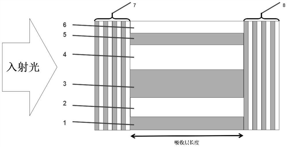
[0021] The implementation of the present invention will be illustrated by specific specific examples below, and those skilled in the art can easily understand other advantages and effects of the present invention from the contents disclosed in this specification.

[0022] Example embodiments will now be described more fully with reference to the accompanying drawings. Example embodiments may, however, be embodied in many forms and should not be construed as limited to the examples set forth herein; rather, these embodiments are provided so that this disclosure will be thorough and complete and fully convey the concept of example embodiments to those skilled in the art. The described features, structures, or characteristics may be combined in any suitable manner in one or more embodiments. In the following description, numerous specific details are provided in order to give a thorough understanding of embodiments of the invention. However, those skilled in the art will apprec...


PUM


Abstract

The invention discloses a high-speed photoelectric detector structure. An epitaxial wafer of the high-speed photoelectric detector structure comprises an InP substrate, a lower ohmic contact layer, a lower window layer, an absorption layer, an upper window layer and an upper ohmic contact layer, the lower ohmic contact layer, the lower window layer, the absorption layer, the upper window layer and the upper ohmic contact layer sequentially grow on the InP substrate from bottom to top, the epitaxial wafer is a mesa structure, and one side surface of the mesa structure is a light incident surface. The incident surface is provided with an antireflection film, the other side surface far away from the antireflection film is a light reflection surface, and the light reflection surface is provided with a high reflection film. A light incident direction of a photodetector is perpendicular to the direction of a drift electric field, the absorption layer is 0.1-3 mu m, the drift of carriers is fast, and a bandwidth is high. While the internal quantum efficiency is improved, the size of the device is further reduced, the bandwidth of the device is improved, the uniform distribution of a photocurrent of the whole absorption layer is balanced, and the problem of nonlinear distortion of signals caused by uneven light absorption of the absorption layer and local photocurrent saturation is avoided.

Description

technical field [0001] The invention relates to the technical field of photodetectors, in particular to a high-speed photodetector and a manufacturing method thereof. Background technique [0002] Optical detectors are widely used in optical communication systems, imaging systems and military fields, and are key optical receiving devices in high-speed optical communication systems. Photodetectors are developing towards high performance and high integration. Optical detectors used in optical fiber communication systems can generally be classified into two types: photodiodes (PDs) and avalanche photodiodes (APDs). The frequency response bandwidth and quantum efficiency of traditional photodetectors restrict each other. Generally, the quantum efficiency of the device can be increased by increasing the absorbing layer of the device, but the transit time of the carriers becomes longer and the response rate decreases. In photodetectors, the absorption of photons occurs in the a...

Claims


Application Information

Patent Timeline
IPC IPC(8): H01L31/0216H01L31/101H01L31/18C23C14/08C23C14/14C23C14/24C23C16/30C23C16/455C23C28/04
CPCY02P70/50
Inventor 陈阳华张永单智发方天足
Owner 全磊光电股份有限公司
Why Eureka
Try Eureka