Epitaxial wafer of ultraviolet light emitting diode and preparation method thereof

A technology of light-emitting diodes and epitaxial wafers, applied in the direction of electrical components, circuits, semiconductor devices, etc.

Active Publication Date: 2021-04-20
HC SEMITEK SUZHOU
View PDF6 Cites 0 Cited by
  • Summary
  • Abstract
  • Description
  • Claims
  • Application Information

AI Technical Summary

Problems solved by technology

[0004] In the process of realizing the present disclosure, the inventors have found that there are at least the following problems in the related

Method used


Image

  • Epitaxial wafer of ultraviolet light emitting diode and preparation method thereof
  • Epitaxial wafer of ultraviolet light emitting diode and preparation method thereof
  • Epitaxial wafer of ultraviolet light emitting diode and preparation method thereof

Examples


Embodiment Construction

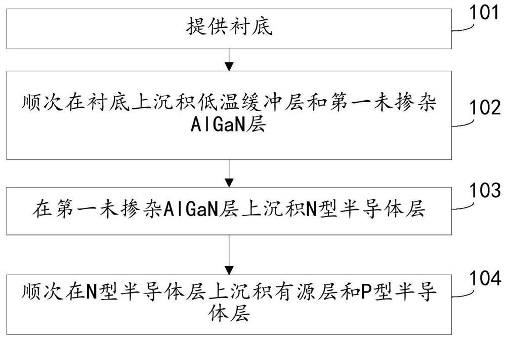
[0039] In order to make the purpose, technical solution and advantages of the present disclosure clearer, the implementation manners of the present disclosure will be further described in detail below in conjunction with the accompanying drawings.

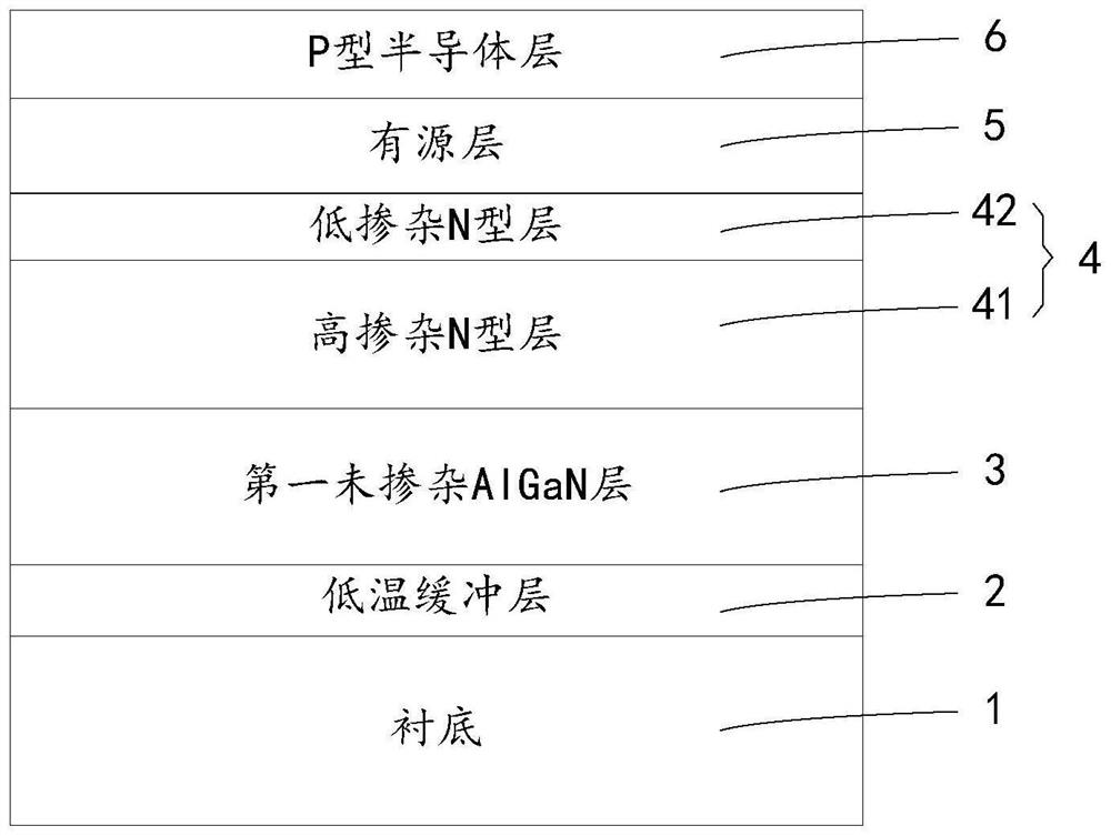
[0040] figure 1 It is a structural schematic diagram of an epitaxial wafer of an ultraviolet light emitting diode provided by an embodiment of the present disclosure. see figure 1 , the epitaxial wafer includes: a substrate 1 and a low-temperature buffer layer 2 , a first undoped AlGaN layer 3 , an N-type semiconductor layer 4 , an active layer 5 and a P-type semiconductor layer 6 stacked on the substrate 1 in sequence.

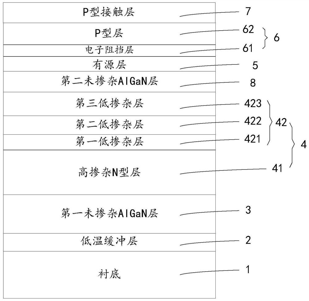
[0041] The N-type semiconductor layer 4 includes a highly doped N-type layer 41 and a low-doped N-type layer 42 sequentially stacked on the first undoped AlGaN layer 3 .

[0042] The low-doped N-type layer 42 includes a first low-doped layer 421 laminated on the highly-doped N-type layer 41 .

[0043] Both the ...


PUM

PropertyMeasurementUnit
Doping concentrationaaaaaaaaaa

Abstract

The invention provides an epitaxial wafer of an ultraviolet light emitting diode and a preparation method thereof, and belongs to the field of light emitting diodes. The epitaxial wafer comprises a substrate, and a low-temperature buffer layer, a first undoped AlGaN layer, an N-type semiconductor layer, an active layer and a P-type semiconductor layer which are sequentially stacked on the substrate, and the N-type semiconductor layer comprises a high-doped N-type layer and a low-doped N-type layer. Wherein the low-doped N-type layer comprises a first low-doped layer stacked on the high-doped N-type layer, the high-doped N-type layer and the first low-doped layer each comprise a plurality of AlGaN layers and a plurality of SiN layers which are distributed alternately, and the Si doping concentration in the high-doped N-type layer is higher than that in the low-doped N-type layer. The electrical property of the ultraviolet light emitting diode can be improved.

Description

technical field [0001] The disclosure relates to the field of light-emitting diodes, in particular to an epitaxial wafer of an ultraviolet light-emitting diode and a preparation method thereof. Background technique [0002] Ultraviolet LED (Light Emitting Diode, light-emitting diode) has broad market application prospects, such as ultraviolet (abbreviated as UV) LED phototherapy instrument is a very popular medical device in the future, but UV LED technology is still in the growth stage, and the internal quantum efficiency is low. This restricts the further development of AlGaN-based UV LEDs. [0003] The related technology provides an epitaxial wafer of an AlGaN-based ultraviolet light emitting diode, the structure of which includes: a substrate and a buffer layer, an N-type layer, an active layer, an electron blocking layer and a P-type layer grown on the substrate in sequence. [0004] During the process of realizing the present disclosure, the inventors found that there...

Claims


Application Information

Patent Timeline
IPC IPC(8): H01L33/02H01L33/00
Inventor 乔楠李昱桦刘旺平刘源
Owner HC SEMITEK SUZHOU
Why Eureka
Try Eureka