Corrosion method for reducing defects on back surface of germanium substrate wafer
A technology for germanium substrates and wafers, which is applied in the field of germanium semiconductor substrate processing, can solve the problems of severe reaction between corrosion liquid and substrate wafers, high requirements for experience techniques, and reduced wafer thickness, so as to achieve enhanced cleaning and stripping effects and reduce experience. Requirements, Effects of Simplified Operations
- Summary
- Abstract
- Description
- Claims
- Application Information
AI Technical Summary
Problems solved by technology
Method used
Image
Examples
Embodiment 1
[0031]The composition of the corrosion is: hydrofluoric acid: nitric acid: hydrogen peroxide: ice acetic acid: bromin = 400: 650: 80: 400: 6, the proportion is a volume ratio. Mass concentration of 49% hydrofluoric acid, nitric acid concentration of 68 mass% concentration of hydrogen peroxide of 30% concentration was 99.7% glacial acetic acid, bromine concentration of 99.5%.
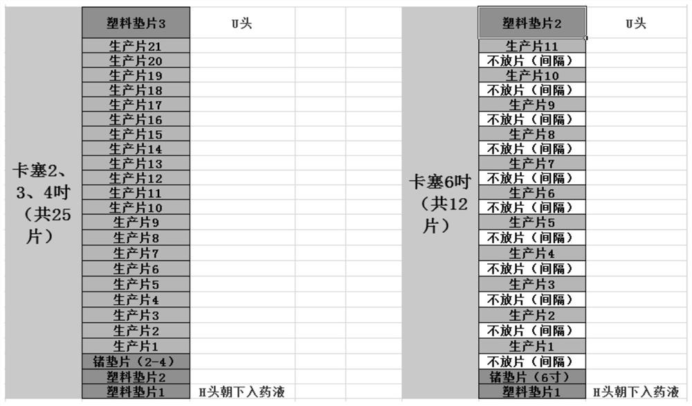
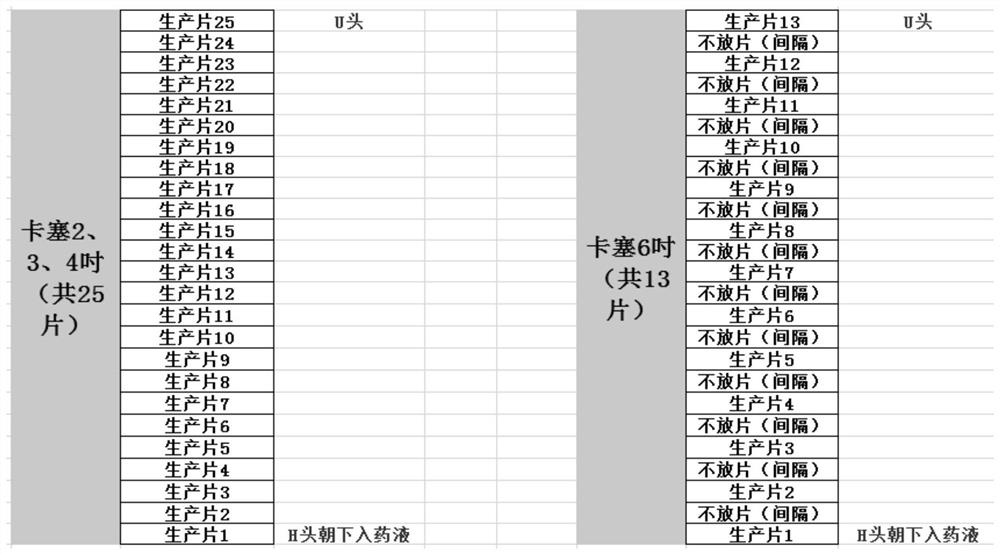
[0032]Corrosion 4 吋 锗 substrate wafer: such asfigure 1 As shown, on the first two slots of the j head in the first two slots, the h-headed striped gasket is inserted into the third slot, and the U head is first slot. Insert a Teflon plastic gasket, and the slot of the slot in the slot of the card is inserted with a ruthenium substrate wafer, and 21 bonge substrate wafers are inserted in each squad.figure 1 The production piece refers to the miter substrate wafer.
[0033]After immersing the Case H, after the corrosion liquid was immersed 5, it was rapidly removed, and it was placed in a flushing tank filled with dei...
Embodiment 2
[0037]Corrosion 6 吋 锗 substrate wafer: such asfigure 1 As shown, the jump is on the first slot in the first slot in the first slot, and the head is inserted in the second slot in the second slot, and the third slot of the h head is not The slice is inserted in the first slot in the first slot, and a 11-piece substrate wafer is inserted in each trial, and there is an empty part of each adjacent two ruthenium substrate wafers. Slot. The remaining references will be 0% from the back surface defect rate; each wafer is uniform, and the strength is not less than 21bf (the thickness is about 280 um).
PUM
 Abstract
Description
Claims
Application Information

