Multi-device combined three-dimensional atom probe sample universal interface device

A technology of atomic probe and universal interface, which is applied in measuring devices, material analysis using wave/particle radiation, and material analysis using radiation, etc. It can solve problems such as poor resolution, inability to operate double-tilt, and low success rate. Achieve the effect of improving detection efficiency, reducing damage rate and low maintenance cost

Active Publication Date: 2021-05-11
SHANGHAI UNIV
View PDF10 Cites 2 Cited by
  • Summary
  • Abstract
  • Description
  • Claims
  • Application Information

AI Technical Summary

Problems solved by technology

However, the information given by the transmission electron microscope is two-dimensional projection, that is, the atomic-level component resolution achieved by the transmission electron microscope is actually two-dimensional, and the resolution along the incident direction of the electron beam is poor.
Therefore, although scientists have used various methods to improve the three-dimensional spatial resolution of the transmission electron microscope in recent years, these methods are still immature and limited by various specific conditions. The best three-dimensional spatial resolution is only about 1nm
[0004]The combination of three-dimensional atom probe technology and transmission electron microscope can realize the characterization of the structure and composition in the nanometer space of materials, but there is still an analysis area Problems with small, difficult orientation relationships
[0008]1. It is necessary to customize a dedicated TEM sample holder, which is extremely expensive;
[0009]2. The operation is inconvenient, the nano needle tip is easily damaged during the sample installation process, and the success rate is very low;
[0010]3. The TEM sample shaft cannot be tilted at a large angle, nor can it be tilted at a large angle. The crystal structure and orientation information of the tip cannot obtain the three-dimensional high-resolution image of the nano-tip, and the results of the transmission electron microscope and the three-dimensional atom probe are not true three-dimensional space fitting

Method used


Image

  • Multi-device combined three-dimensional atom probe sample universal interface device
  • Multi-device combined three-dimensional atom probe sample universal interface device
  • Multi-device combined three-dimensional atom probe sample universal interface device

Examples


Embodiment 1

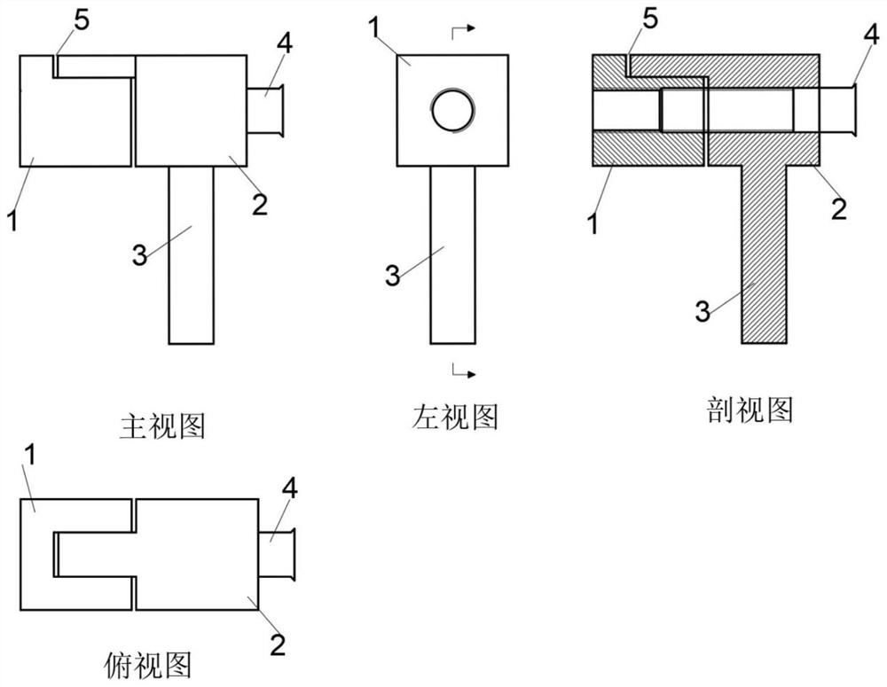
[0032] In this example, see Figure 1-3 , a three-dimensional atom probe sample universal interface device used in combination with multiple devices, including a needle-point sample support platform, a common sample platform matching platform and a sample transfer part, the needle-point sample support platform is installed on the common sample platform matching platform, and the sample The transfer part fixes the ordinary sample stage matching stage;

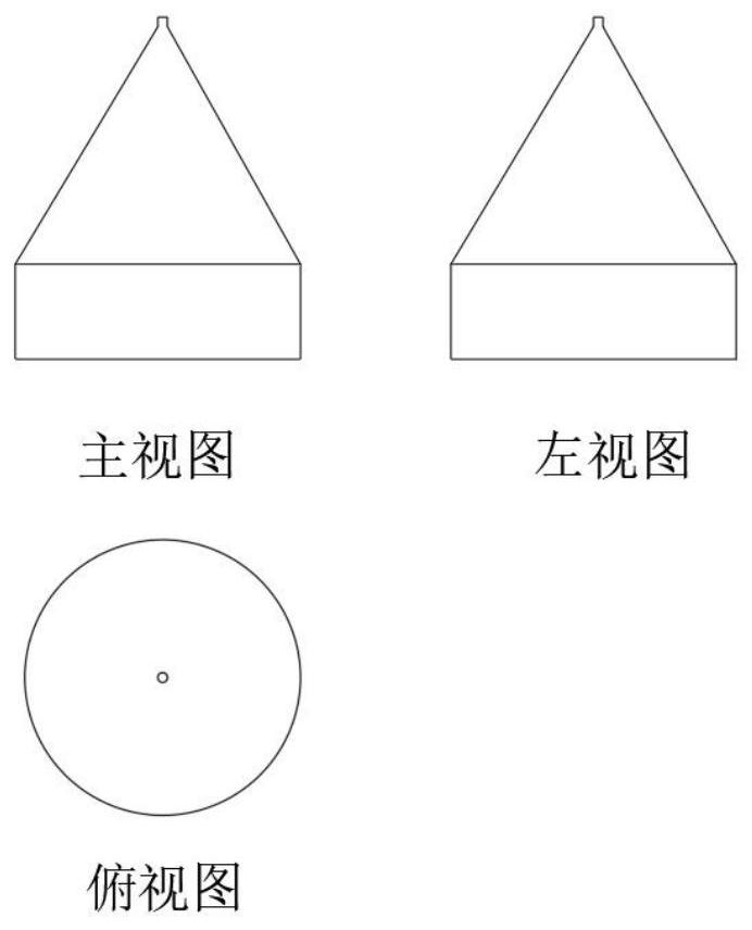
[0033] The pinpoint sample support platform is in the shape of a cone, and the needlepoint sample is welded to the top of the cone tip of the needlepoint sample support platform;

[0034] The matching table of the ordinary sample stage is in the shape of a ball table, and the matching table of the ordinary sample stage is welded together with at least two pinpoint sample support platforms, and is used as an ordinary sample stage directly placed on TEM, SEM, EBSD or TKD equipment;

[0035] The lower part of the sample transfer par...

Embodiment 2

[0040] This embodiment is basically the same as Embodiment 1, especially in that:

[0041] In this example, see figure 1 , a universal interface device for three-dimensional atom probe samples used by multiple devices. The needle-point sample support platform is integrally formed by a conical part and a cylindrical part. The bottom of the conical part is connected with the end of the cylindrical part. The thickness of the cylindrical part is 0.1-0.2mm, the cross-sectional size of the cylindrical part is 0.2-0.3mm, the height of the conical part is 0.3-0.4mm, the top of the conical part is truncated, the cross-sectional size is not more than 10μm, and the truncated The height of the tip of the cone is not less than 10 μm.

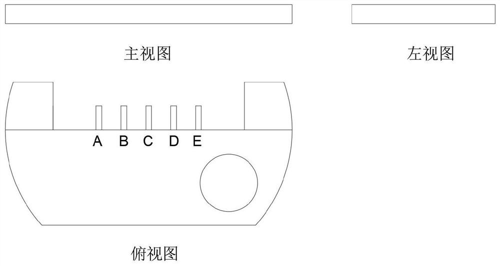
[0042] In this example, see figure 2 The thickness of the ball table shape of the ordinary sample table matching table is 0.1-0.2mm, and the diameter is not more than 3mm. At least 5 support frames are set on one side of the ball table shape, and the need...

Embodiment 3

[0048] This embodiment is basically the same as the previous embodiment, and the special features are:

[0049] In this embodiment, the common sample stage matching stage such as figure 2 As shown, it is semicircular, with five positions A, B, C, D, and E on it. It can weld the transmission sample cut by FIB and the needle-point sample support platform. The needle-point sample support platform is as follows figure 1 shown. The needle-point sample support table can weld the three-dimensional atom probe needle-point sample. Ordinary sample stage matching stage can be directly placed in transmission electron microscope, scanning electron microscope, double focused ion beam and other equipment for direct observation, realizing the equipment linkage of SEM-TEM-FIB-TKD-EBSD. When observing the tip sample of the three-dimensional atom probe, the screw of the sample transfer table is first rotated outward, leaving a certain gap between the groove of the sample transfer table and th...


PUM

PropertyMeasurementUnit
thicknessaaaaaaaaaa
sizeaaaaaaaaaa
heightaaaaaaaaaa

Abstract

The invention discloses a multi-device combined three-dimensional atom probe sample universal interface device, which comprises a needle tip sample supporting table, a common sample table matching table and a sample switching part, the needle tip sample supporting table is arranged on the common sample table matching table, and the sample switching part is used for fixing the common sample table matching table. The device is used in combination with microscopic structure analysis instruments such as a scanning electron microscope, an EBSD-TKD, a transmission electron microscope, a focused ion beam, a three-dimensional atom probe and the like. According to the invention, transmission electron microscope analysis, scanning electron microscope analysis, focused ion beam analysis, EBSD or TKD analysis of a three-dimensional atom probe tip sample are realized by using a plurality of microscopic structures to analyze an original common sample table. The device is simple in structure, convenient to process and maintain and extremely low in cost, double inclination of the sample can be realized in the transmission electron microscope, the tip sample of the three-dimensional atom probe can be directly observed in different microscopic structure analysis instruments, and advantage complementation of various instruments and equipment is realized.

Description

technical field [0001] The invention relates to a multi-device universal sample interface for observing a three-dimensional atom probe tip sample, which belongs to an accessory used in a multi-dimensional and multi-scale characterization method of information such as the morphology, composition, and structure of nano-micro regions of materials. Background technique [0002] The three-dimensional atom probe equipment is composed of time-of-flight mass spectrometer, position sensitive probe and control field evaporation system and other components. The atoms on the surface of the tip sample with a radius of curvature less than 100nm are ionized under the action of a strong electric field, the field evaporates away from the sample surface, and fly to the position-sensitive probe. Recording the flight time can realize the identification of ion species one by one, so as to obtain various elements in the material nanometer The three-dimensional distribution in space and the abilit...

Claims


Application Information

Patent Timeline
Patent Type & Authority Applications(China)
IPC IPC(8): G01N23/04G01N23/2251G01N23/2204G01N23/20025H01J37/20H01J37/28
CPCG01N23/04G01N23/2251G01N23/2204G01N23/20025H01J37/20H01J37/28
Inventor 李慧张孟超刘文庆梁雪彭剑超寇春合
Owner SHANGHAI UNIV
Why Eureka
Try Eureka