Vertical charge transfer type photon demodulator and working method thereof

A technology of charge transfer and working method, applied in the field of photonic demodulators, can solve the problems of shallow field area, shallow depletion area, and reduced efficiency, and achieve the effects of fast switching, good high frequency response and modulation ratio

Pending Publication Date: 2021-05-11
南京威派视半导体技术有限公司 +1
View PDF1 Cites 1 Cited by
  • Summary
  • Abstract
  • Description
  • Claims
  • Application Information

AI Technical Summary

Problems solved by technology

[0003] The CAPD device invented by Sony in patent US 8,294,882 B2 has simple process, high sensitivity, high quantum efficiency, and fast speed. Shallow, greatly reducing efficiency
The PMD technology adopted by Infineon uses photo-gate to generate depletion region for photosensitivity. There is also the problem that as the pixel size shrinks, the depletion region becomes shallower, which eventually leads to a decrease in quantum efficiency.
There is still no small-sized ToF device that can maintain high sensitivity and quantum efficiency

Method used


Image

  • Vertical charge transfer type photon demodulator and working method thereof
  • Vertical charge transfer type photon demodulator and working method thereof
  • Vertical charge transfer type photon demodulator and working method thereof

Examples


Embodiment Construction

[0037] The present invention is described in further detail now in conjunction with accompanying drawing. These drawings are all simplified schematic diagrams, which only illustrate the basic structure of the present invention in a schematic manner, so they only show the configurations related to the present invention.

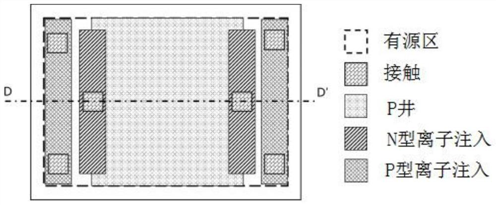
[0038] figure 1 It is a schematic diagram of the layout of a single pixel of the vertical charge transfer photon demodulator of the present invention, wherein each layout: the dotted line frame AA is an active area, indicating that this area has no shallow trench isolation or isolation of insulating materials such as deep trenches; CT is a contact, Indicates that the position is used as the metal contact of the electrode; TPW is P-type well implantation for horizontal isolation; SN is heavily doped N-type ion implantation; SP is heavily doped P-type ion implantation.

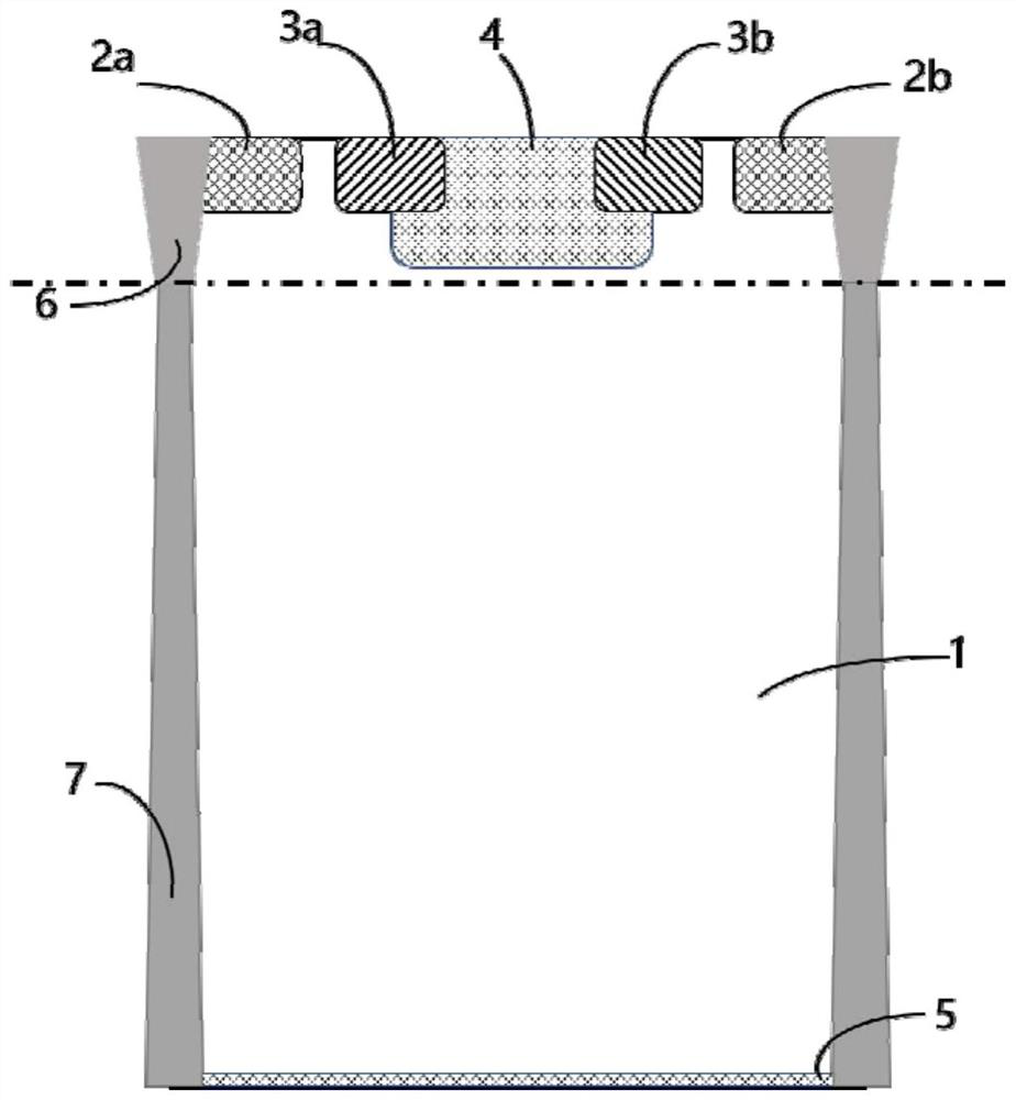
[0039] figure 1 The section diagram along DD’ in the middle is a single-pixel structure di...


PUM

PropertyMeasurementUnit
Depthaaaaaaaaaa

Abstract

The invention relates to a vertical charge transfer type photon demodulator and a working method thereof. The upper surface of a semiconductor is provided with a modulation-demodulation part, and the lower surface of the semiconductor extends to the bottom of a substrate to form a photosensitive part; the photosensitive part converts photons into photon-generated carriers, photo-generated electron-hole pairs are separated by using a vertical electric field, and electrons or holes are vertically transported to the surface of a semiconductor for optical signal demodulation. The two charge collection regions are 1.8 V, the modulation switch I is connected with 1.2 V, the modulation switch II is connected with 0V, the substrate electrode is grounded, a transverse electric field is generated at the upper part of the semiconductor substrate, and a vertical electric field is generated in other regions; photons are absorbed by the semiconductor and excite an electron-hole pair, the electron-hole pair is separated under the action of an electric field, and electrons move upwards to the surface of the semiconductor; and under the action of a transverse electric field, the electrons further move to the vicinity of a charge collection region and enters a depletion region generated by the electrons through diffusion to form a light current signal. The photon demodulator is small in size and high in sensitivity and quantum efficiency.

Description

technical field [0001] The invention relates to a vertical charge transfer photon demodulator, and also relates to a working method of the vertical charge transfer photon demodulator, belonging to the technical field of photon demodulators. Background technique [0002] ToF is widely used as a method of optical ranging, and the main purpose of TOF devices is to be able to read signals with fixed frequency and fixed phase, and a high-speed sensor is required to read the required integration time. The signal within, that is, the sensor has a better response to high-frequency signals. The usual practice is to feed the signal to the desired readout node at the desired time and to the other node at the opposite time. [0003] The CAPD device invented by Sony in patent US 8,294,882 B2 has simple process, high sensitivity, high quantum efficiency, and fast speed. Shallow, greatly reducing efficiency. The PMD technology adopted by Infineon uses photo-gate to generate depletion re...

Claims


Application Information

Patent Timeline
IPC IPC(8): H01L27/146
CPCH01L27/1461H01L27/1463
Inventor 马浩文沈凡翔王子豪王凯李张南顾郅扬胡心怡柴智陈辉常峻淞李龙飞
Owner 南京威派视半导体技术有限公司
Why Eureka
Try Eureka