SiP module based on silicon switching four-layer three-dimensional stacking and manufacturing method

A manufacturing method and switching technology, applied in semiconductor/solid-state device manufacturing, electric solid-state devices, semiconductor devices, etc., can solve the problems of bare chips without considering chip stacking, lack of versatility, and inability to meet the application requirements of SiP products, etc. Achieving the effect of reduced area, good flexibility, and low overall cost

Pending Publication Date: 2021-05-14
XIAN MICROELECTRONICS TECH INST
View PDF9 Cites 4 Cited by
  • Summary
  • Abstract
  • Description
  • Claims
  • Application Information

AI Technical Summary

Problems solved by technology

However, the integration of MCU and special-purpose processing chips makes the system architecture not have strong versatility. At the same time, chip stacking is not cons...

Method used


Image

  • SiP module based on silicon switching four-layer three-dimensional stacking and manufacturing method
  • SiP module based on silicon switching four-layer three-dimensional stacking and manufacturing method
  • SiP module based on silicon switching four-layer three-dimensional stacking and manufacturing method

Examples


Embodiment

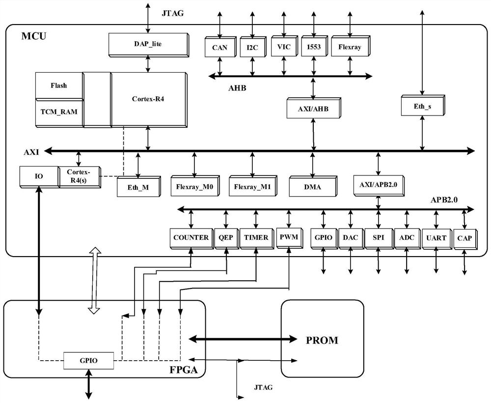
[0053] The first step: system design and simulation:

[0054] Phase 1: According to the system block diagram ( figure 1 ) to carry out the principle design of the SiP module, integrate the MCU, FPGA and PROM of the ARM core into the SiP, and form an embedded minimum system based on MCU+FPGA. The hardware implementation can be divided into two parts, namely MCU part and FPGA and configurable IO part. MCU implements system control, data calculation and peripheral interface control, FPGA implements logic decoding, IO and other function expansion;

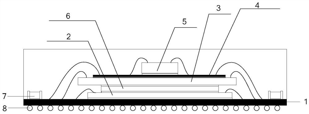
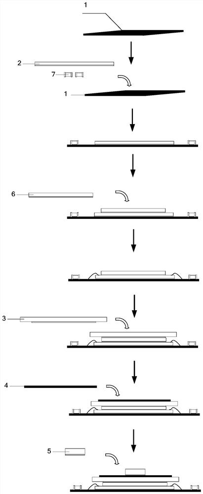
[0055] Phase 2: Carry out the process design of the SiP module, propose a feasible process and packaging scheme, and complete the design of the organic substrate and silicon interposer substrate. The module adopts the packaging process based on the organic substrate, and the multi-chip layout is carried out on the surface of the substrate, and the MCU, FPGA, silicon transfer substrate and PROM are stacked in four layers: bottom, midd...


PUM

PropertyMeasurementUnit
Plate thicknessaaaaaaaaaa
Thicknessaaaaaaaaaa
Thicknessaaaaaaaaaa

Abstract

The invention discloses a SiP module based on silicon switching four-layer three-dimensional stacking and a manufacturing method. Three large-scale integrated circuits are integrated in the SiP module, the application requirement of miniaturization is fully considered in packaging implementation, a four-layer three-dimensional stacking structure based on a silicon switching substrate is adopted, a MCU chip, a FPGA chip, the silicon switching substrate and the PROM chip are stacked in a lower layer, a middle lower layer, a middle upper layer and an upper layer, and SiP packaging is achieved in the modes of adhesive bonding, lead bonding, injection molding and the like. According to the invention, the area is reduced to 15% of the original area; compared with an implementation mode that a bare chip is flatly laid in SiP, the area is reduced to 50% of the original area. According to the invention, for the application requirements of high-integration, generalization, low-cost and modular products, by relying on the nested integration architecture of the MCU and the SiP and the multifunctional pin multiplexing technology, better flexibility and lower overall cost are achieved, and various requirements on the market can be quickly met.

Description

technical field [0001] The invention belongs to the field of SiP modules, and in particular relates to a SiP module based on silicon transfer four-layer three-dimensional stacking and a manufacturing method. Background technique [0002] SiP (System in Package, SiP) is a high-performance module composed of one or more chips and passive devices stacked in a housing in the form of chip dies, so that the package is upgraded from a single chip to a system-on-chip. At present, in military fields such as aviation, aerospace, weapons, and industrial control fields such as oil and gas exploration, nuclear power units, and hybrid vehicles, SiP is favored because of its miniaturization, modularization, high reliability, and localization, and has become the solution to system integration. One of the main ways. [0003] At present, the traditional two-dimensional assembly density of chips has reached the limit, which has limited ability to increase the density of system integrated SiP ...

Claims


Application Information

Patent Timeline
IPC IPC(8): H01L25/16H01L21/98
CPCH01L25/16H01L25/50
Inventor 张越匡乃亮郭雁蓉赵超张盼
Owner XIAN MICROELECTRONICS TECH INST
Why Eureka
Try Eureka