Thin film packaging structure and preparation method thereof, and display panel

A thin-film packaging and substrate technology, which is used in semiconductor/solid-state device manufacturing, electrical components, and electrical solid-state devices, etc., can solve problems such as intrusion and packaging failure, and achieve the effects of easy operation, improved packaging performance, and simple methods.

Pending Publication Date: 2021-06-01
HKC CORP LTD
View PDF5 Cites 3 Cited by
  • Summary
  • Abstract
  • Description
  • Claims
  • Application Information

AI Technical Summary

Problems solved by technology

[0004] The purpose of this application is to provide a thin-film packaging structure and its preparation method, aiming to solve the problem of packaging failure caused by water vapor intruding into the device from the crack after the inorganic layer of the thin-film packaging structure breaks

Method used


Image

  • Thin film packaging structure and preparation method thereof, and display panel
  • Thin film packaging structure and preparation method thereof, and display panel
  • Thin film packaging structure and preparation method thereof, and display panel

Examples


preparation example Construction

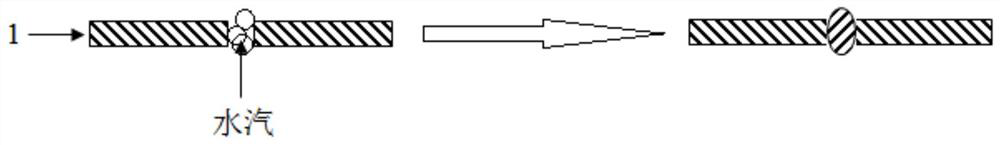
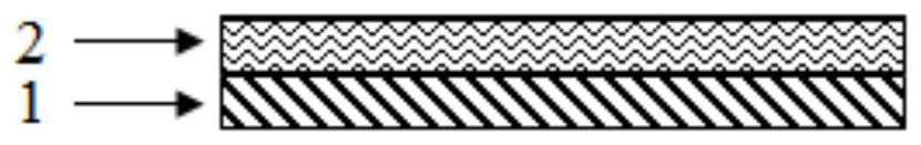
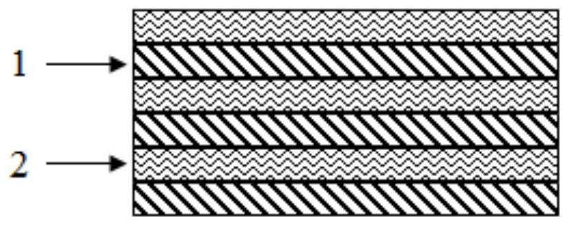
[0055] In order to obtain the above thin film encapsulation structure, the embodiment of the present application also provides a preparation method of the thin film encapsulation structure, the preparation method of the thin film encapsulation structure includes the following steps of preparing an inorganic layer:

[0056] S01, performing film-forming treatment on the inorganic slurry to obtain an inorganic layer;

[0057] Wherein, the inorganic slurry includes a water-swellable material or a precursor for forming the water-swellable material, and the water-swellable material includes at least one of sodium bentonite, nano-scale silica gel, and ettringite.

[0058] In the preparation method of the thin film encapsulation structure provided in the embodiment of the present application, the inorganic slurry including the water-absorbing swellable material or the precursor used to form the water-absorbing swellable material is subjected to film-forming treatment, so as to obtain a...


PUM

PropertyMeasurementUnit
thicknessaaaaaaaaaa
thicknessaaaaaaaaaa
thicknessaaaaaaaaaa

Abstract

The invention belongs to the technical field of display, and particularly relates to a thin film packaging structure and a preparation method thereof, and a display panel. The thin film packaging structure provided by the invention comprises an inorganic layer, wherein a material for forming the inorganic layer comprises a water-absorbing expansion material, and the water-absorbing expansion material comprises at least one selected from the group consisting of sodium bentonite, nanoscale silica gel and ettringite. When the inorganic layer is fractured to generate cracks in a production process or a use process, the water-absorbing expansion material at the cracks absorbs invaded water vapor to expand, so the cracks are filled, self-repairing of the inorganic layer is completed, the invaded water vapor is consumed, repairing of the cracks is completed, the water vapor is effectively prevented from invading the interior of a device along the cracks, the packaging performance of the thin film packaging structure is improved, and the service life of a display device is prolonged.

Description

technical field [0001] The present application belongs to the field of display technology, and in particular relates to a thin film encapsulation structure, a preparation method thereof, and a display panel. Background technique [0002] In recent years, organic light-emitting diode (Organic Light-Emitting Diode, OLED) has become a very popular emerging flat-panel display device product at home and abroad, because OLED display device has self-illumination, wide viewing angle, short response time, high luminous efficiency, wide color Domain, low operating voltage, thin thickness, large-size and flexible panels can be produced, and the process is simple, and it also has the potential of low cost. [0003] Since the OLED display unit will be corroded and damaged under the action of water vapor and oxygen, it is very important to adopt a suitable packaging technology. In the encapsulation of the OLED display unit, a thin film encapsulation structure including an inorganic layer...

Claims


Application Information

Patent Timeline
Patent Type & Authority Applications(China)
IPC IPC(8): H01L51/52H01L51/56H01L27/32
CPCH10K59/10H10K50/846H10K50/844H10K71/00
Inventor 唐榕聂军张建英袁海江
Owner HKC CORP LTD
Why Eureka
Try Eureka