Gallium nitride device and driving circuit thereof

A gallium nitride and device technology, applied in circuits, semiconductor devices, electronic switches, etc., can solve problems such as device performance needs to be improved, it is difficult to ensure circuit system failure safety, unfavorable drive circuit design, etc.

Active Publication Date: 2021-06-08
HUAWEI TECH CO LTD
View PDF7 Cites 1 Cited by
  • Summary
  • Abstract
  • Description
  • Claims
  • Application Information

AI Technical Summary

Problems solved by technology

[0003] The normally-on GaN device needs a stable on-current to keep it on, and a reverse voltage must be applied to the gate to turn off the device. This characteristic is not conducive to the design of the drive circuit. , and the power consumption of the device is high; in addit

Method used


Image

  • Gallium nitride device and driving circuit thereof
  • Gallium nitride device and driving circuit thereof
  • Gallium nitride device and driving circuit thereof

Examples


Embodiment Construction

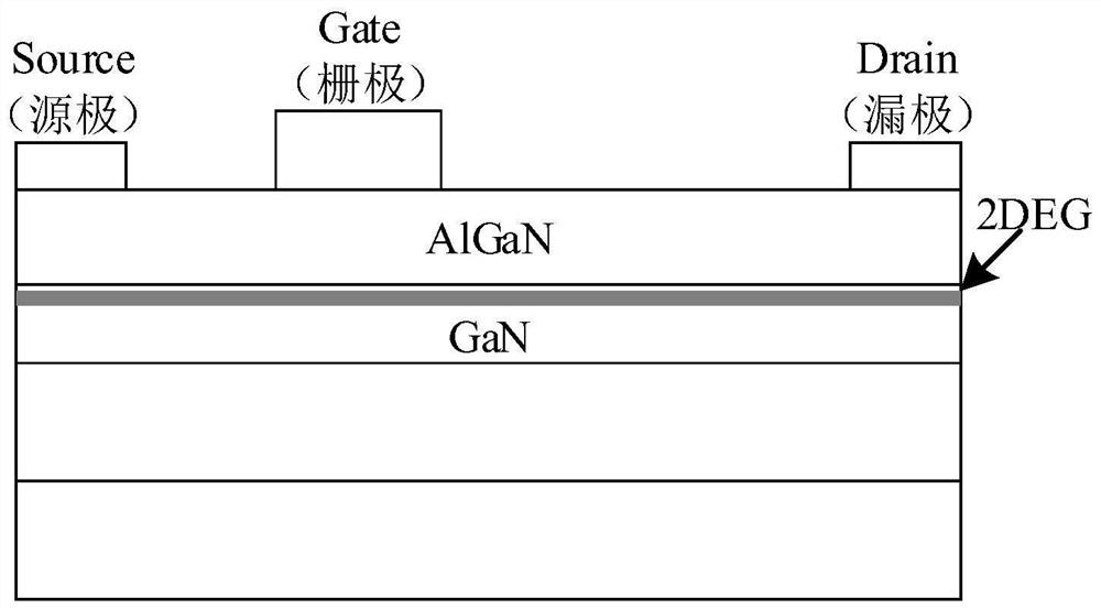
[0027] Gallium nitride (GaN, gallium nitride) is a compound of nitrogen and gallium. It is a semiconductor with direct energy gaps of Group III (boron group elements) and group V (nitride group elements). Gallium nitride has a wide energy gap. It is 3.4eV (electron volts), and the energy gap of silicon, the most commonly used semiconductor material today, is 1.12eV, so gallium nitride has better performance than silicon devices in high-power and high-speed devices.

[0028] Energy gap (band gap or energy gap): also known as energy band gap (energy band gap), width of forbidden band (width of forbidden band), generally refers to the energy gap from the top of the valence band to the bottom of the conduction band of a semiconductor or insulator. Among them, direct band gaps (direct band gaps) refer to the energy band structure in which the minimum value of the bottom of the conduction band and the maximum value of the top of the valence band of the semiconductor material correspo...


PUM


Abstract

The invention discloses a gallium nitride device and a driving circuit thereof. The gallium nitride device comprises: a substrate (100); a gallium nitride (GaN) buffer layer (200) formed on the substrate (100); an AlGaN (AlGaN) barrier layer (300) formed on the GaN buffer layer (200); the source electrode (S), the drain electrode (D) and the grid electrode are formed on the AlGaN barrier layer (300); wherein the grid electrode comprises a P-type doped gallium nitride P-GaN cover layer (400) formed on the AlGaN barrier layer (300), and first grid electrode metal (M1) and second grid electrode metal (M2) formed on the P-GaN cover layer (400), Schottky contact is formed between the first grid electrode metal (M1) and the P-GaN cover layer (400), and ohmic contact is formed between the second grid electrode metal (M2) and the P-GaN cover layer (400). The gallium nitride device is a normally-closed device, so that the design of a driving circuit is facilitated; moreover, the gallium nitride device is provided with a mixed gate structure composed of a Schottky gate and an ohmic gate, so that the gate electric leakage in the conduction process can be reduced, the driving power consumption is reduced, a large number of holes can be injected into the AlGaN barrier layer during conduction, the dynamic resistance is optimized, and the reliability of the device is improved.

Description

technical field [0001] The present application relates to the technical field of semiconductors, in particular to a gallium nitride device and a driving circuit thereof. Background technique [0002] With the development of power products towards high efficiency and miniaturization, GaN devices such as power switches based on GaN, a wide bandgap semiconductor material, have attracted more and more attention. At present, GaN devices mainly include devices based on aluminum gallium nitride / gallium nitride (AlGaN / GaN) lateral heterostructures, which can naturally form a two-dimensional electron gas (two-dimensional electron gas) with high electron mobility at its interface. -dimensional electron gas, 2DEG) channel. Generally speaking, the 2DEG at the interface of the heterostructure is difficult to be depleted under normal circumstances, so that the current gallium nitride devices based on the AlGaN / GaN heterostructure are usually normally-on devices. [0003] The normally-on...

Claims


Application Information

Patent Timeline
IPC IPC(8): H01L29/778H01L29/423H01L29/45H01L29/47
CPCH01L29/778H01L29/42316H01L29/452H01L29/475H01L29/7786H01L29/2003H01L29/1066H01L29/205H03K17/284
Inventor 黄伯宁侯召政蒋其梦
Owner HUAWEI TECH CO LTD
Why Eureka
Try Eureka