Production method and device of heterogeneous deep groove PiN array and silicon-based reconfigurable stealth antenna
A deep groove and array technology, applied in the field of devices and silicon-based reconfigurable stealth antennas, can solve the problems of antenna stealth performance reduction, difficult antenna performance dynamic reconfiguration, etc., achieve concentration and distribution improvement, improve system integration and stealth Performance, effect of improved concentration and uniformity of distribution
- Summary
- Abstract
- Description
- Claims
- Application Information
AI Technical Summary
Problems solved by technology
Method used
Image
Examples
Embodiment 1
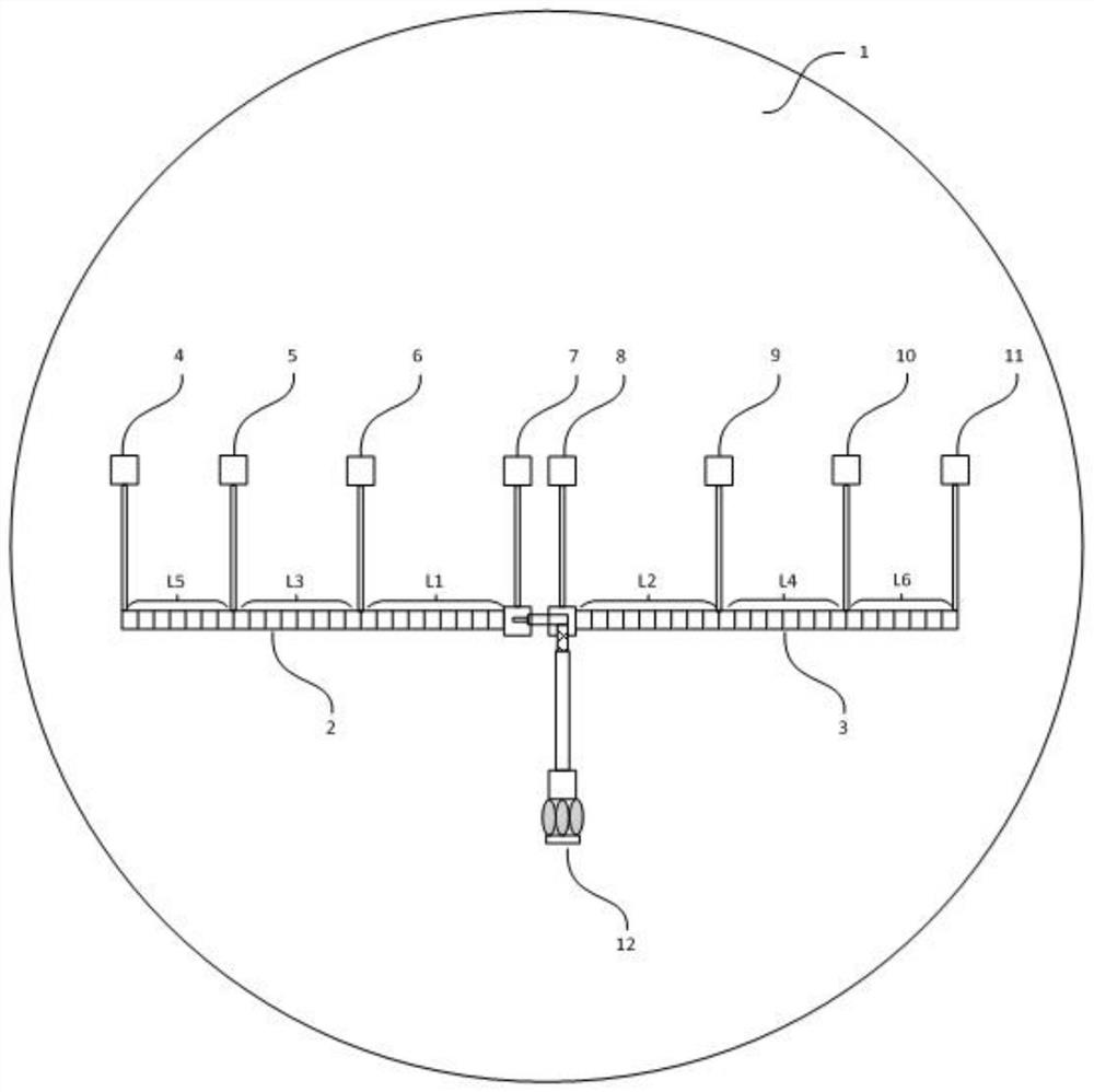
[0062] See figure 1 , figure 1 It is a structural schematic diagram of a silicon-based reconfigurable stealth antenna according to an embodiment of the present invention. The silicon-based reconfigurable stealth antenna includes: a semiconductor substrate 1, a first antenna arm 2, a second antenna arm 3, a first DC bias line 4, a second DC bias line 5, a third DC bias line Line 6, the fourth DC bias line 7, the fifth DC bias line 8, the sixth DC bias line 9, the seventh DC bias line 10, the eighth DC bias line 11, and the coaxial feeder line 12; The antenna arm is composed of multiple heterogeneous deep trench protected PiN diode array units.
[0063] The silicon-based reconfigurable stealth antenna includes a first antenna arm and a second antenna arm. The antenna arm includes a plurality of heterogeneous deep groove PiN array units, and the antenna performance is realized by controlling the on and off of different PiN diode array units. Reconfiguration; the number of diod...
Embodiment 2
[0112] See Figure 3a-Figure 3t , Figure 3a-Figure 3t It is a schematic diagram of a preparation method of a heterogeneous deep trench PiN array according to an embodiment of the present invention. On the basis of the first embodiment above, the preparation of a deep trench protection PiN diode array with a solid-state plasma region length of 90 microns is taken as an example to describe in detail. The length of the intrinsic region can be between 50 microns and 150 microns, and the specific steps are as follows:
[0113] S10, selecting a GeOI substrate.
[0114] See Figure 3a , the crystal orientation of the GeOI substrate 101 may be (100) or (110) or (111), without any limitation here. In addition, the doping type of the GeOI substrate 101 can be n-type or p-type, and the doping concentration is, for example, 0.5×10 14 ~1×10 15 cm -3 , the thickness of the top layer Ge is, for example, 30-120 μm.
[0115] S20, doping into the GeOI substrate to form a top-layer GeSn ...
Embodiment 3
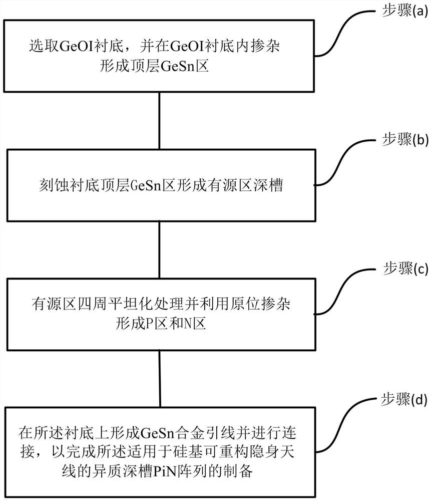
[0154] Please refer to Figure 4 , Figure 4 It is a schematic diagram of a device structure of a GaAs-GeSn-GaAs heterogeneous deep trench protection PiN diode according to an embodiment of the present invention. The silicon-based deep trench protected PiN diode adopts the above-mentioned as figure 2 prepared as indicated. Specifically, the heterogeneous GeSn-based silicon-based deep groove protection PiN diode is prepared and formed on the GeOI substrate 301, and the P region 303, the N region 304 of the diode, and the local area between the P region 303 and the N region 304 in the lateral direction. The constitutive regions are located in the GeSn region 302 of the top layer of the GeOI substrate.
[0155] Please refer to Figure 5 , Figure 5 It is a schematic structural diagram of a heterogeneous deep trench PiN array according to an embodiment of the present invention. The heterogeneous deep groove PiN array is composed of silicon-based solid-state plasma antenna b...
PUM
| Property | Measurement | Unit |
|---|---|---|
| thickness | aaaaa | aaaaa |
Abstract
Description
Claims
Application Information


