Light-emitting diode epitaxial wafer and growth method thereof

A technology of light-emitting diodes and growth methods, applied in the field of light-emitting diode epitaxial wafers and their growth, can solve the problems of reducing the luminous efficiency of light-emitting diodes, affecting the wavelength consistency of epitaxial wafers, and affecting the incorporation of multiple quantum well layers, so as to ensure consistent wavelengths performance, ensure normal operation, and improve luminous efficiency

Active Publication Date: 2022-04-12
HC SEMITEK SUZHOU
View PDF12 Cites 0 Cited by
  • Summary
  • Abstract
  • Description
  • Claims
  • Application Information

AI Technical Summary

Problems solved by technology

[0004] Due to the difference in lattice constant between substrate (silicon carbide, sapphire, silicon wafer, etc.) The incorporation of In will affect the wavelength uniformity of the epitaxial wafer and reduce the luminous efficiency of the light-emitting diode.

Method used


Image

  • Light-emitting diode epitaxial wafer and growth method thereof
  • Light-emitting diode epitaxial wafer and growth method thereof
  • Light-emitting diode epitaxial wafer and growth method thereof

Examples


Embodiment Construction

[0037] In order to make the purpose, technical solution and advantages of the present disclosure clearer, the implementation manners of the present disclosure will be further described in detail below in conjunction with the accompanying drawings.

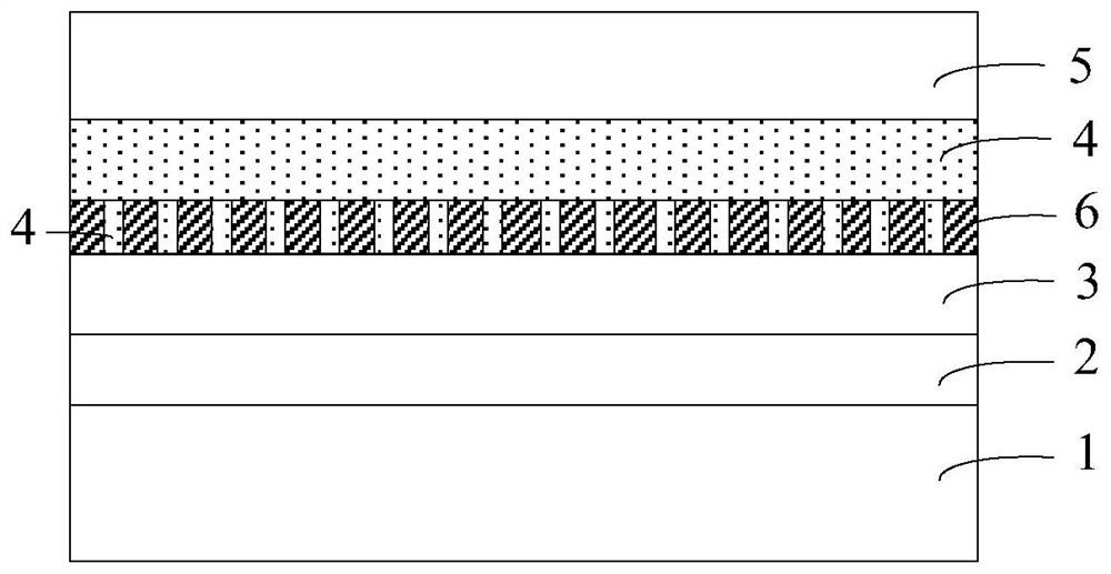
[0038] figure 1 is a schematic structural view of a light-emitting diode epitaxial wafer provided by an embodiment of the present disclosure, as shown in figure 1 As shown, the light-emitting diode epitaxial wafer includes a substrate 1 , and a gallium nitride buffer layer 2 , an N-type semiconductor layer 3 , a multi-quantum well layer 4 and a P-type semiconductor layer 5 stacked on the substrate 1 in sequence.

[0039] The multiple quantum well layer 4 is prepared by molecular beam epitaxy. The light-emitting diode epitaxial wafer also includes SiO disposed between the N-type semiconductor layer 3 and the multi-quantum well layer 4 2 Thin film layer6. MQW layer 4 imprinted on SiO 2 On the thin film layer 6, and part of the mu...


PUM

PropertyMeasurementUnit
thicknessaaaaaaaaaa
thicknessaaaaaaaaaa
thicknessaaaaaaaaaa

Abstract

The disclosure provides a light-emitting diode epitaxial wafer and a growth method thereof, belonging to the technical field of semiconductors. The light-emitting diode epitaxial wafer includes a substrate, and a gallium nitride buffer layer, an N-type semiconductor layer, a multi-quantum well layer and a P-type semiconductor layer sequentially stacked on the substrate, and the multi-quantum well layer is made of molecular prepared by beam epitaxy, the light emitting diode epitaxial wafer also includes SiO disposed between the N-type semiconductor layer and the multiple quantum well layer 2 thin film layer, the MQW layer is imprinted on the SiO 2 On the thin film layer, and part of the multi-quantum well layer passes through the SiO 2 The thin film layer is in contact with the N-type semiconductor layer. The epitaxial wafer can ensure the wavelength consistency of the epitaxial wafer and the luminous efficiency of the light emitting diode.

Description

technical field [0001] The present disclosure relates to the technical field of semiconductors, in particular to a light-emitting diode epitaxial wafer and a growth method thereof. Background technique [0002] A light-emitting diode (English: Light Emitting Diode, referred to as: LED) is a semiconductor electronic component that can emit light. As an efficient, environmentally friendly and green new solid-state lighting source, LED is a new generation of light source with broad prospects, and is being rapidly and widely used in traffic lights, car interior and exterior lights, urban landscape lighting, indoor and outdoor display screens and small-pitch displays. screen and other fields. [0003] The epitaxial wafer is the main component of the LED. The existing GaN-based LED epitaxial wafer includes a substrate and a buffer layer stacked on the substrate in sequence, an undoped GaN layer, an N-type layer, a multi-quantum well layer and a P-type layer. layer. The N-type l...

Claims


Application Information

Patent Timeline
Patent Type & Authority Patents(China)
IPC IPC(8): H01L33/06H01L33/00
CPCH01L33/06H01L33/0062
Inventor 王群郭炳磊葛永晖董彬忠李鹏
Owner HC SEMITEK SUZHOU
Why Eureka
Try Eureka