Multi-feed packaging antenna based on fan-out packaging

An antenna and feeder technology, applied in the field of multi-feed packaged antennas, to achieve the effect of eliminating loss, realizing beam performance and wide beam performance

Active Publication Date: 2021-06-22
CHINA ELECTRONIC TECH GRP CORP NO 38 RES INST
View PDF6 Cites 2 Cited by
  • Summary
  • Abstract
  • Description
  • Claims
  • Application Information

AI Technical Summary

Problems solved by technology

[0006] Aiming at the deficiencies of the prior art, the present invention provides a multi-feed packaged antenna based on fan-out packaging, which solves the problem of how to realize the chip multi-port power combining function on the packaged antenna

Method used


Image

  • Multi-feed packaging antenna based on fan-out packaging
  • Multi-feed packaging antenna based on fan-out packaging
  • Multi-feed packaging antenna based on fan-out packaging

Examples


Embodiment 1

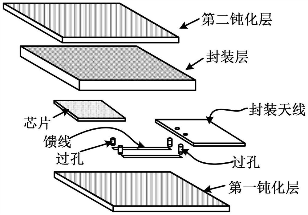
[0049] like figure 1 As shown, taking the double-fed packaged antenna as an example, the implementation process of this embodiment is described in detail:

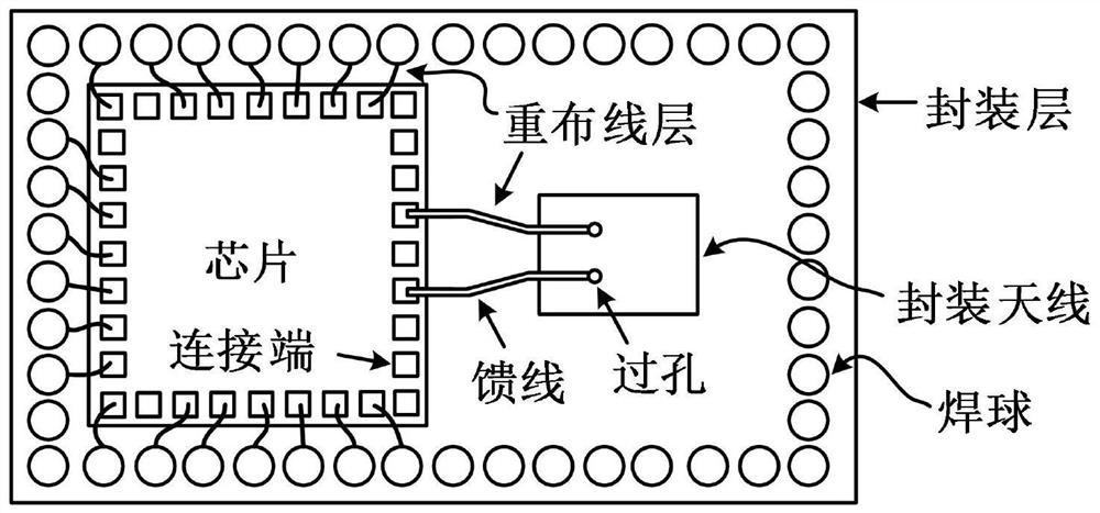
[0050] Doubly-fed package antenna based on fan-out package, including package layer, chip and package antenna;

[0051] The chip is a millimeter wave chip, the chip is embedded in the packaging layer, the chip is embedded in the packaging layer, and the side where the chip connection terminal is located is exposed, for example, the lower end surface of the chip and the lower end surface of the packaging layer are located on the same plane.

[0052] Considering that in the traditional fan-out packaging process, the packaging layer adopts plastic packaging, and the physical performance of the chip is improved by using a thicker packaging material on top of the chip. However, the plastic packaging material used in fan-out packaging has high processing costs and high loss, and has a higher curvature than glass, and in the mill...

Embodiment 2

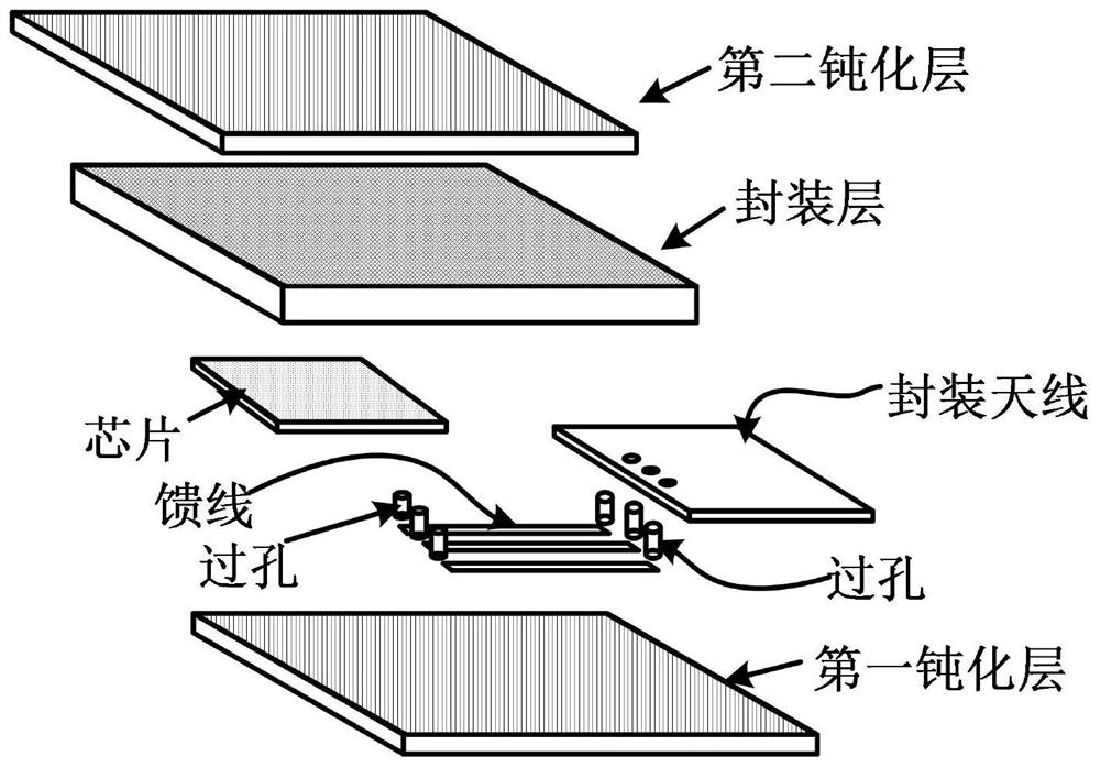
[0065] like image 3 As shown, taking the three-feed packaged antenna as an example, the implementation process of this embodiment will be described in detail:

[0066] Doubly-fed package antenna based on fan-out package, including package layer, chip and package antenna;

[0067] Doubly-fed package antenna based on fan-out package, including package layer, chip and package antenna;

[0068] The chip is a millimeter wave chip, the chip is embedded in the packaging layer, the chip is embedded in the packaging layer, and the side where the chip connection terminal is located is exposed, for example, the lower end surface of the chip and the lower end surface of the packaging layer are located on the same plane.

[0069] Considering that in the traditional fan-out packaging process, the packaging layer adopts plastic packaging, and the physical performance of the chip is improved by using a thicker packaging material on top of the chip. However, the plastic packaging material u...


PUM


Abstract

The invention provides a multi-feed packaging antenna based on fan-out packaging, and relates to the technical field of packaging antennas. According to the invention, the first passivation layer is arranged below the packaging layer, and the first re-wiring layer and the second re-wiring layer are arranged on the first passivation layer to complete the multi-feed packaging antenna structure. Connection ends of a plurality of channels of a chip are connected to an antenna feed structure of a packaged antenna, a metal layer where the antenna feed structure is located is completed by a first rewiring layer in package, and a second rewiring layer is mainly used for realizing the packaged antenna. Due to the fact that a coaxial feed mode is adopted, namely two rewiring layers are used, the multi-port power synthesis function can be achieved on the antenna; meanwhile, the characteristics of loss and small working bandwidth brought by a lossy power synthesizer can be eliminated, the working bandwidth and the beam bandwidth of the antenna are almost as wide as those of a single antenna, and the antenna has the advantages of being simple in structure and convenient to use. Therefore, the size and the cost of the system can be effectively reduced, and the equivalent omnidirectional radiation power of the system is improved.

Description

technical field [0001] The invention relates to the technical field of packaged antennas, in particular to a fan-out package-based multi-feed packaged antenna. Background technique [0002] In the millimeter wave or even terahertz frequency band, since the operating wavelength reaches the millimeter or submillimeter level, it is possible to integrate the package antenna and the millimeter wave chip. Antenna-in-Package (AIP) is based on packaging technology and materials, and integrates the millimeter wave chip and antenna in the packaging structure, which can better take into account the size, performance and cost of the antenna, so as to better realize the microsystem Level wireless transmission function. [0003] Fan-Out Wafer Level Packaging (FOWLP), in the wafer manufacturing process, pulls out the required circuit from the terminal of the semiconductor die to the redistribution layer (Redistribution Layer), and then forms package, the cost is relatively cheap. Existi...

Claims


Application Information

Patent Timeline
Patent Type & Authority Applications(China)
IPC IPC(8): H01Q1/38H01Q1/50H01Q9/04H01L23/66H01L23/31
CPCH01Q1/38H01Q1/50H01Q9/0407H01L23/66H01L23/3107H01L2223/6677H01Q1/2283H01Q1/40H01L2224/04105H01L2224/12105H01L2223/6627H01L2224/24195H01L24/20H01L24/16H01L24/24H01L24/25H01L24/73H01L2224/16225H01L2224/24265H01L2224/25171H01L2224/73209
Inventor 朱传明段宗明戴跃飞
Owner CHINA ELECTRONIC TECH GRP CORP NO 38 RES INST
Why Eureka
Try Eureka