

Groove type power device and manufacturing method thereof
A technology for power devices and manufacturing methods, which is applied in the manufacture of semiconductor/solid-state devices, semiconductor devices, electric solid-state devices, etc. Effect of Stabilizing Threshold Voltage and Breakdown Voltage
- Summary
- Abstract
- Description
- Claims
- Application Information
AI Technical Summary
Problems solved by technology
Method used
Image

Examples
Embodiment 1
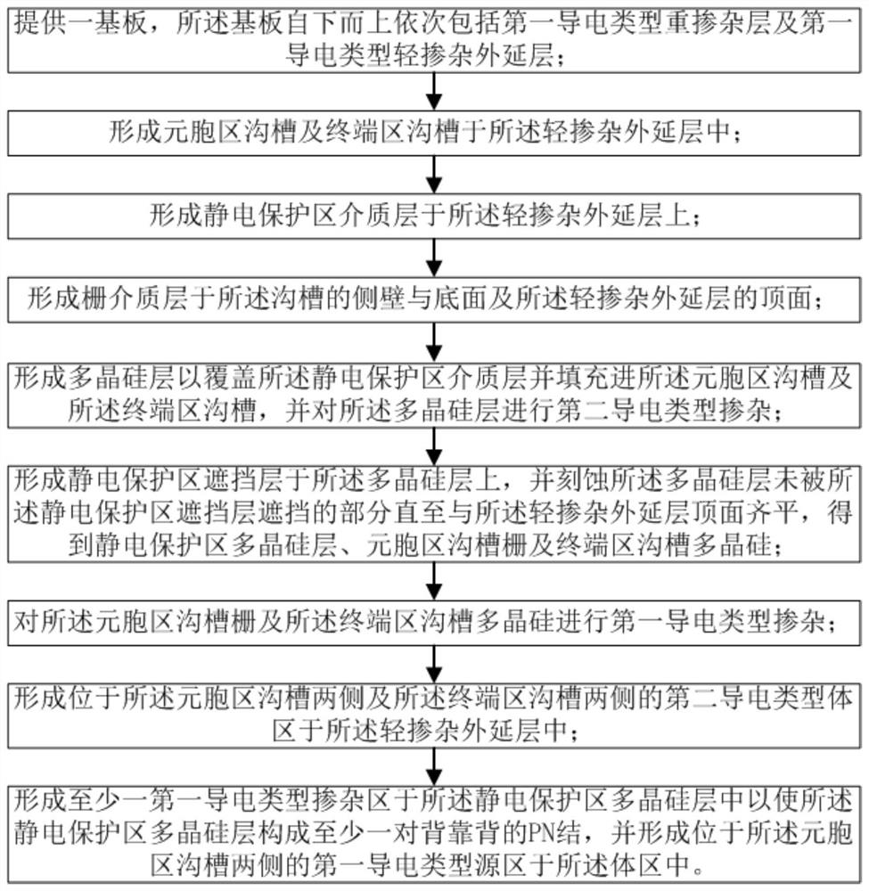
[0103] In this embodiment, a method for manufacturing a trench power device is provided, please refer to figure 1 , shown as a process flow diagram of the method, comprising the following steps:
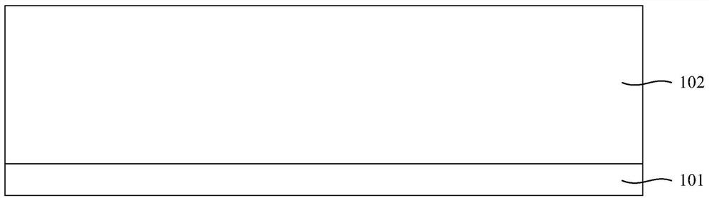
[0104] see figure 2 , providing a substrate, the substrate sequentially includes a first conductivity type heavily doped layer 101 and a first conductivity type lightly doped epitaxial layer 102 from bottom to top.
[0105] As an example, the first conductivity type may be N-type or P-type. When the first conductivity type is N-type, the following second conductivity type is correspondingly P-type. When the first conductivity type When it is P-type, the following second conductivity type is correspondingly N-type. In this embodiment, the heavily doped layer 101 of the first conductivity type takes N-type heavily doped silicon as an example, the lightly doped epitaxial layer 102 of the first conductivity type takes N-type silicon as an example, and the first conductivity type The ...
Embodiment 2
[0140] A trench type power device is provided in this embodiment, please refer to Figure 18 , is shown as a cross-sectional structure diagram of the device, including a substrate, a trench in the cell region, a trench in the terminal region, a dielectric layer 107a in an electrostatic protection region, a gate dielectric layer 108, a polysilicon layer 109a in an electrostatic protection region, and a cell region of the first conductivity type Trench gate 109b, trench polysilicon 109c in the terminal region of the first conductivity type, body region 111 of the second conductivity type and source region 112b of the first conductivity type, wherein the substrate includes heavily doped first conductivity type in sequence from bottom to top layer 101 and the lightly doped epitaxial layer 102 of the first conductivity type; the trenches in the cell region and the trenches in the terminal region are located in the lightly doped epitaxial layer 102; the dielectric layer 107a in the e...
PUM
| Property | Measurement | Unit |
|---|---|---|
| Thickness | aaaaa | aaaaa |
| Thickness | aaaaa | aaaaa |
| Thickness | aaaaa | aaaaa |
Abstract
Description
Claims
Application Information