Method for polishing silicon wafer
A grinding method and technology for silicon wafers, which are used in grinding machine tools, grinding devices, manufacturing tools, etc.
- Summary
- Abstract
- Description
- Claims
- Application Information
AI Technical Summary
Problems solved by technology
Method used
Image

Examples
Embodiment 1
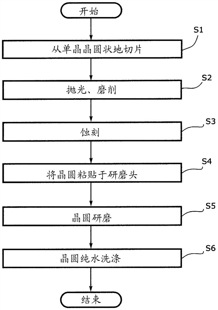
[0045] In Example 1, according to image 3 In the shown flow, a single-side mirror polishing process is performed on a silicon wafer having a diameter of 300 mm.
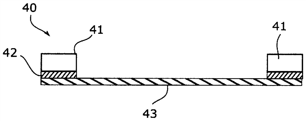
[0046] The material of the retaining ring 3 is glass epoxy resin, and the washing of the retaining ring is, as an alkali wash, in SC1 (NH 4 OH: 1wt%, H 2 O 2 : 1 wt% mixed solution) immersed for 30 minutes, and then rinsed with pure water. In addition, as pickling, it was immersed in HF (1 wt %) for 30 minutes, pickled, and then rinsed with pure water.
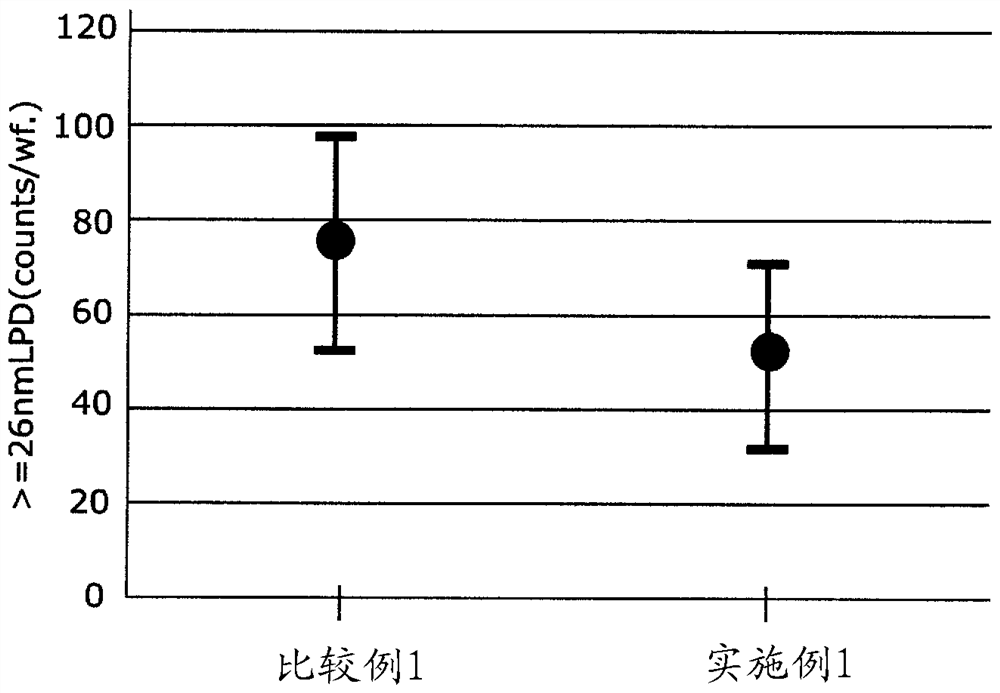
[0047] The number of particles on the front side of the polished silicon wafer was measured with a laser scattering particle counter (Surfscan SP-3 manufactured by KLA-Tencor).
PUM
 Abstract
Description
Claims
Application Information
 - R&D
- Intellectual Property
- Life Sciences
- Materials
- Tech Scout
- Unparalleled Data Quality
- Higher Quality Content
- 60% Fewer Hallucinations
Browse by: Latest US Patents, China's latest patents, Technical Efficacy Thesaurus, Application Domain, Technology Topic, Popular Technical Reports.
© 2025 PatSnap. All rights reserved.Legal|Privacy policy|Modern Slavery Act Transparency Statement|Sitemap|About US| Contact US: help@patsnap.com