Semiconductor packaging structure
A packaging structure, semiconductor technology, applied in the direction of semiconductor devices, semiconductor/solid-state device components, electrical solid-state devices, etc., can solve problems such as DRAM electrostatic damage
- Summary
- Abstract
- Description
- Claims
- Application Information
AI Technical Summary
Problems solved by technology
Method used
Image

Examples
Embodiment Construction
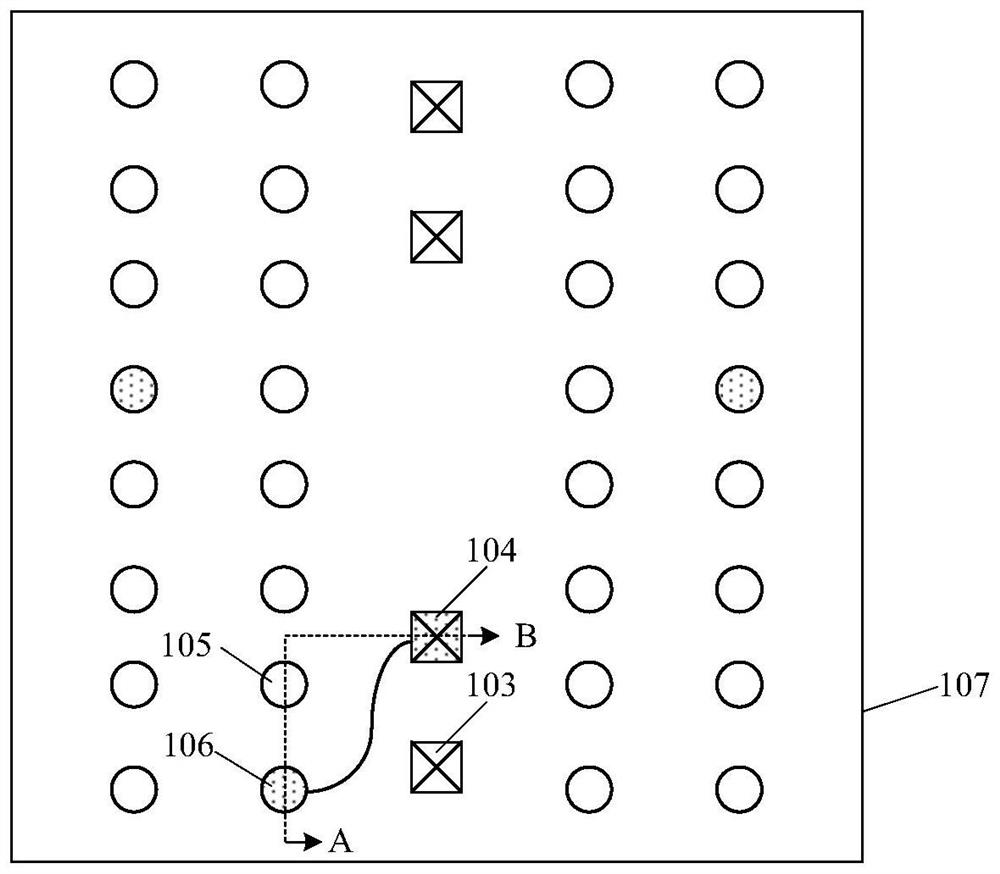
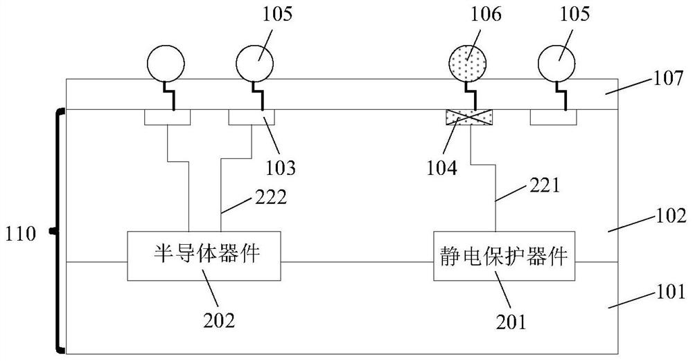
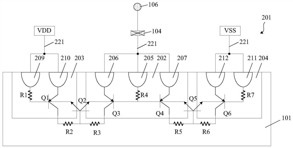
[0024] As mentioned in the background art, the DRAM packaged in a ball grid array (BGA, Ball Grid Array) usually causes electrostatic damage.
[0025] Research has found that the current specific process of packaging DRAM in the form of a ball grid array (BGA, Ball Grid Array) includes: forming an integrated circuit corresponding to the DRAM memory on a semiconductor substrate and forming a number of circuits connected to the integrated circuit. Welding pads; forming several pins connected to the several pads, the pins may be solder balls; forming a plastic sealing layer for plastic sealing the integrated circuit, and the plastic sealing layer exposes part of the surface of the pins. In order to ensure that the stress of the packaging structure is uniform during packaging, when forming normal pins connected to the pads, it is also necessary to form a number of floating dummy pins as required (the dummy pins are not in contact with the formed integrated circuit and soldering pad...
PUM
 Abstract
Description
Claims
Application Information
 - R&D
- Intellectual Property
- Life Sciences
- Materials
- Tech Scout
- Unparalleled Data Quality
- Higher Quality Content
- 60% Fewer Hallucinations
Browse by: Latest US Patents, China's latest patents, Technical Efficacy Thesaurus, Application Domain, Technology Topic, Popular Technical Reports.
© 2025 PatSnap. All rights reserved.Legal|Privacy policy|Modern Slavery Act Transparency Statement|Sitemap|About US| Contact US: help@patsnap.com