Two-dimensional Van der Waals bipolar transistor based on tellurium nanosheets and construction method thereof

A bipolar transistor, tellurium nanotechnology, applied in the manufacture of transistors, semiconductor devices, semiconductor/solid-state devices, etc., can solve the problems of poor performance of BJTs, the problem of electrode contact is not considered, and the service performance of unstable devices, etc. Effects of strong thickness dependence, stable p-type semiconductor properties, good air stability

Active Publication Date: 2021-07-16
UNIV OF SCI & TECH BEIJING
View PDF2 Cites 2 Cited by
  • Summary
  • Abstract
  • Description
  • Claims
  • Application Information

AI Technical Summary

Problems solved by technology

Two-dimensional MoS constructed by Liu et al. 2 / WSe 2 / MoS 2 NPN type BJTs common emitter current gain (β) is 12 (Adv.Funct.Mater.2019, 1807893), but due to WSe 2 It has the characteristics of bipolar electrical transport (both holes and electrons participate in conduction), and it is not a perfect two-dimensional p-type semiconductor material. The diode rectification effect is not very good, resulting in poor performance of BJTs; Sikandar et al. use two-dimensional BP / MoS 2 The PNP-type BJTs built with / BP heterostructure have a β value of about 10.1 at room temperature (2D Mater.6(2019) 035005), and the current amplification factor is still far from the industrial-grade requirements (20-200).
This is the first attempt based on two-dimensional PNP-type BJTs, but the electrode contact problem has not been considered, and the instability of BP also threatens the service performance of the device

Method used


Image

  • Two-dimensional Van der Waals bipolar transistor based on tellurium nanosheets and construction method thereof
  • Two-dimensional Van der Waals bipolar transistor based on tellurium nanosheets and construction method thereof
  • Two-dimensional Van der Waals bipolar transistor based on tellurium nanosheets and construction method thereof

Examples


Embodiment 1

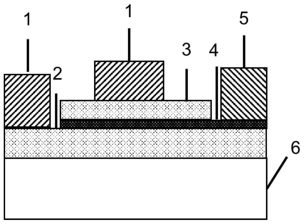
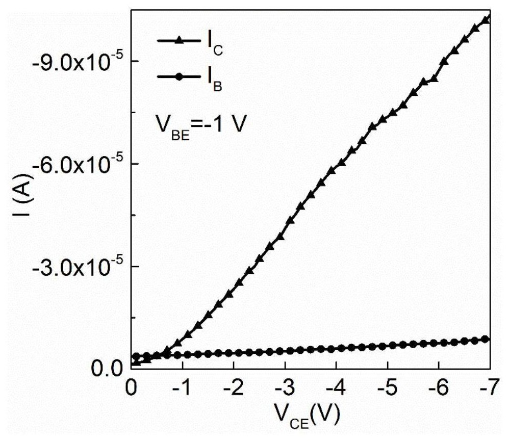
[0078] like figure 1 As shown, a two-dimensional van der Waals bipolar transistor based on tellurium nanosheets includes 1 high work function metal electrode, 2 thick layer tellurium nanosheets, 3 thin layer tellurium nanosheets, 4 two-dimensional n-type semiconductor materials, 5 low work function Functional metal electrodes, 6 target substrates;

[0079]Wherein, the thick-layer tellurium nanosheet 2 is covered on the target substrate 6; the two-dimensional n-type semiconductor material 4 is covered on the surface of the thick-layer tellurium nanosheet 2, and the regions 2-4 are emitter junctions for emitting electrons; The thin-layer tellurium nanosheet 3 covers the surface 4 of the two-dimensional n-type semiconductor material, and the regions 3-4 are collector junctions for collecting electrons; the high work function metal electrode 1 is arranged on the thick-layer tellurium nanosheet 2 and On the surface of the thin-layer tellurium nanosheet 3, the electrode 1 is Au wit...

Embodiment 2

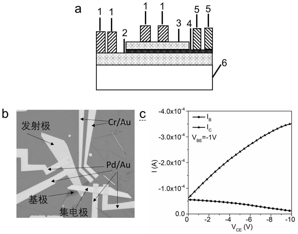
[0091] The device structure of the two-dimensional van der Waals bipolar transistor based on tellurium nanosheets in this example is basically the same as that in Example 1, except that the preparation process and transfer method of the two-dimensional n-type semiconductor are different, and the number of electrodes is upgraded to two deposited on the surface of each material. .

[0092] like figure 1 As shown, a two-dimensional van der Waals bipolar transistor based on tellurium nanosheets includes 1 high work function metal electrode Pd / Au (thickness is 5nm / 70nm), 2 thick layers of tellurium nanosheets (thickness is 30nm), 3 thin layers Tellurium nanosheets (thickness is 5.5nm), 4 molybdenum disulfide (thickness is 3nm), 5 low work function metal electrode Cr / Au (thickness is 5nm / 50nm), 6 target substrate (300nm thick insulating silicon substrate);

[0093] Wherein, the thick-layer tellurium nanosheet 2 is covered on the target substrate 6; the molybdenum disulfide 4 is cov...


PUM

PropertyMeasurementUnit
thicknessaaaaaaaaaa
thicknessaaaaaaaaaa
thicknessaaaaaaaaaa

Abstract

The invention discloses a two-dimensional Van der Waals bipolar transistor based on tellurium nanosheets and a construction method thereof, and belongs to the technical field of semiconductor materials. The two-dimensional Van der Waals bipolar transistor (BJTs) based on the tellurium nanosheets comprises two-dimensional p-type tellurium nanosheets with different thicknesses, a two-dimensional n-type semiconductor material, an electrode and a target substrate. The tellurium nanosheets with different thicknesses and the two-dimensional n-type semiconductor nanosheets are synthesized by adopting a hydrothermal method, the carrier concentration difference is regulated and controlled by changing the thicknesses of the tellurium nanosheets of a collector electrode and an emitter electrode, the tunneling potential barrier of carriers is regulated and controlled by changing the thickness of a two-dimensional n-type semiconductor of a base electrode, vertical lossless stacking of three layers of materials is achieved by means of PPC auxiliary transfer, a p-type semiconductor is designed to be in contact with high-work-function metal, and the n-type semiconductor is designed to be in contact with low-work-function metal, so that a Schottky barrier between the metal and the material is reduced, the performance of BJTs is effectively regulated and controlled, and a good current amplification function is achieved.

Description

technical field [0001] The invention relates to the technical field of semiconductor materials, in particular to a two-dimensional van der Waals bipolar transistor based on tellurium nanosheets and a construction method thereof. Background technique [0002] With the increasing integration of semiconductor devices, bipolar transistors (BJTs) play a more important role in high-speed digital integrated circuits for large computers, precision analog circuits, and amplifier circuits for radio communications. However, BJTs based on traditional semiconductors (Si, Ge) require complex manufacturing processes, such as the need to use high-energy ion implantation doping to obtain high carrier concentration, control the interface and thickness at the atomic scale, and so on. As devices continue to shrink, problems such as lattice mismatch, dislocation defects, interdiffusion, and cross-contamination become more and more significant. Therefore, it is difficult to reduce the thickness o...

Claims


Application Information

Patent Timeline
Patent Type & Authority Applications(China)
IPC IPC(8): H01L29/73H01L29/737H01L29/06H01L29/267H01L21/34
CPCH01L29/7308H01L29/7311H01L29/737H01L29/0607H01L29/0684H01L29/0665H01L29/267H01L29/66969
Inventor 张跃于慧慧张铮高丽张先坤洪孟羽曾浩然柳柏杉肖建坤汤文辉李瑞山
Owner UNIV OF SCI & TECH BEIJING
Why Eureka
Try Eureka