Quantum dot light-emitting diode and preparation method thereof
A quantum dot light-emitting and diode technology, which is applied in the manufacture of semiconductor/solid-state devices, electrical components, electric solid-state devices, etc., can solve the problems of low light-emitting efficiency of quantum-dot light-emitting diodes, improve device light-emitting efficiency, increase injection concentration, The effect of increasing the chance of compounding
- Summary
- Abstract
- Description
- Claims
- Application Information
AI Technical Summary
Problems solved by technology
Method used
Image
Examples
Embodiment 1
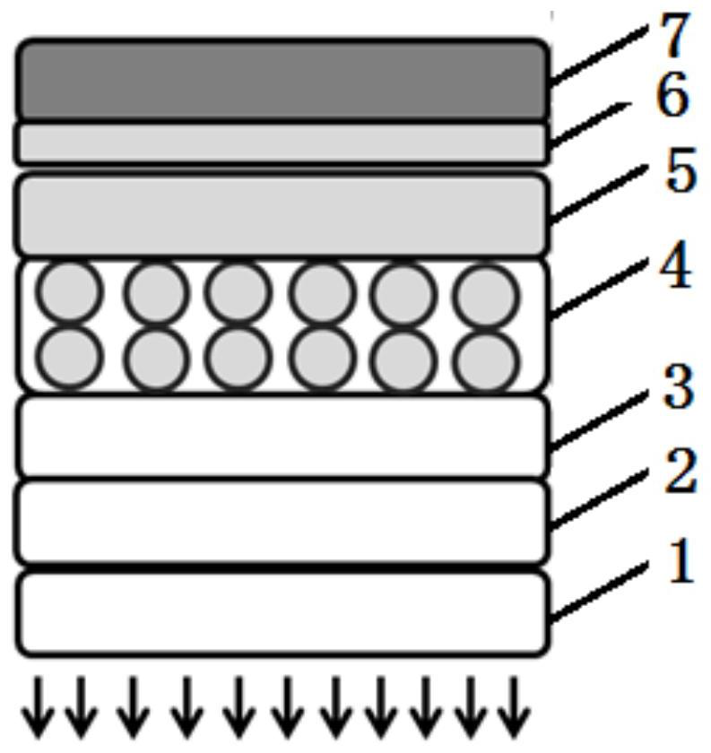
[0044] The preparation steps of the quantum dot light-emitting diode are as follows:
[0045] First, the patterned ITO substrate was placed in acetone, washing solution, deionized water, and isopropanol in sequence for ultrasonic cleaning, and each step of ultrasonic cleaning lasted for about 15 minutes. After the ultrasound is completed, place the ITO substrate in a clean oven to dry for later use;
[0046] After the ITO substrate is dried, treat the surface of the ITO substrate with UV-ozone for 5 minutes to further remove the organic matter attached to the surface of the ITO substrate and improve the work function of the ITO substrate;
[0047] Then, deposit a layer of hole injection layer PEDOT:PSS on the ITO substrate processed in the previous step. done in air;
[0048] Next, place the dried substrate coated with the hole injection layer in a nitrogen atmosphere, spin-coat a layer of hole transport layer material TFB, the thickness of this layer is 30nm, and place the ...
Embodiment 2
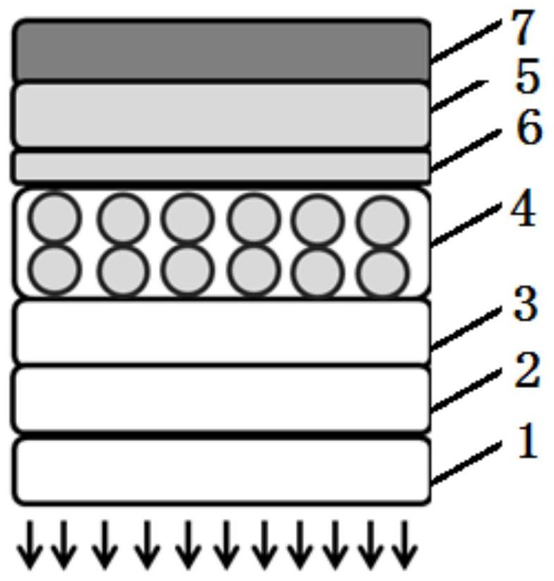
[0055] The preparation steps of the quantum dot light-emitting diode are as follows:
[0056] First, the patterned ITO substrate is placed in acetone, washing solution, deionized water and isopropanol in sequence for ultrasonic cleaning, and each step of ultrasonic cleaning needs to last for about 15 minutes. After the ultrasound is completed, place the ITO substrate in a clean oven to dry for later use;
[0057] After the ITO substrate is dried, treat the surface of the ITO substrate with UV-ozone for 5 minutes to further remove the organic matter attached to the surface of the ITO substrate and improve the work function of the ITO substrate;
[0058] Then, deposit a layer of hole injection layer PEDOT:PSS on the ITO substrate processed in the previous step. done in air;
[0059] Next, place the dried substrate coated with the hole injection layer in a nitrogen atmosphere, spin-coat a layer of hole transport layer material TFB, the thickness of this layer is 30nm, and place...
PUM
| Property | Measurement | Unit |
|---|---|---|
| Thickness | aaaaa | aaaaa |
| Thickness | aaaaa | aaaaa |
Abstract
Description
Claims
Application Information


