Blue-light perovskite thin film, preparation thereof, and inverted quasi-two-dimensional blue-light perovskite light-emitting diode

A light-emitting diode and perovskite technology, which is applied in semiconductor/solid-state device manufacturing, semiconductor devices, electrical components, etc., can solve the problems of spectral red shift, poor stability, and low device performance, and achieve improved grain refinement, improved Thin film morphology, the effect of suppressing the blue shift of the spectrum

Active Publication Date: 2021-07-16
SOUTH CHINA UNIV OF TECH
View PDF4 Cites 5 Cited by
  • Summary
  • Abstract
  • Description
  • Claims
  • Application Information

AI Technical Summary

Problems solved by technology

However, there are few reports on flip-chip blue perovskite light-emitting diodes
This is due to deprotonation and too many defects, resulting in spectral red shift, low device performance and poor stability

Method used


Image

  • Blue-light perovskite thin film, preparation thereof, and inverted quasi-two-dimensional blue-light perovskite light-emitting diode
  • Blue-light perovskite thin film, preparation thereof, and inverted quasi-two-dimensional blue-light perovskite light-emitting diode
  • Blue-light perovskite thin film, preparation thereof, and inverted quasi-two-dimensional blue-light perovskite light-emitting diode

Examples


Embodiment 1

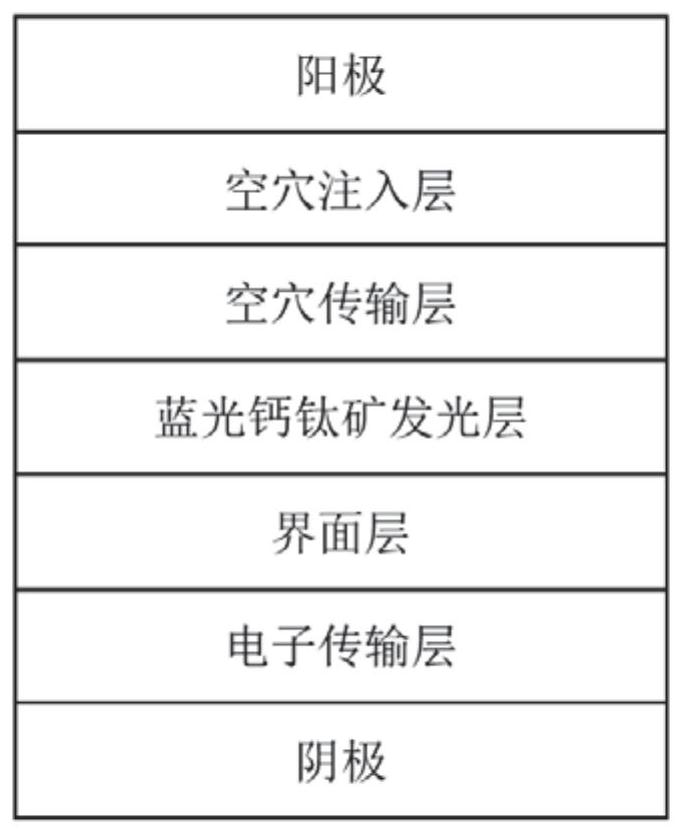
[0061] The device structure of the flip-chip quasi-two-dimensional blue light perovskite light-emitting diode of this embodiment is: cathode (ITO) / electron transport layer (ZnO) / interface layer (PEIE) / blue light perovskite light emission with a peak wavelength of emission spectrum of 490nm layer / hole transport layer (TFB) / hole injection layer (MoO 3 ) / anode (A1).

[0062] The preparation process is as follows:

[0063] a. Prepare the solution: use DMSO to sequentially dissolve PbBr 2 , F-PEABr (p-fluorophenethylamine bromide, F-Ph-CH 2 CH 2 NH 3 Br, 1,4 substitution on the benzene ring) and CsBr are formulated into a solution to obtain a blue light perovskite precursor solution; PbBr in the blue light perovskite precursor solution 2 The concentration of F-PEABr is 0.2mmol / mL, the concentration of F-PEABr is 0.25mmol / mL, and the concentration of CsBr is 0.1mmol / mL;

[0064] b. O 2 -Plasma treatment to improve wettability on ITO, transfer substrate into N 2 In the glove ...

Embodiment 2

[0071] The device structure of the present embodiment is: cathode (ITO) / electron transport layer (ZnO) / interface layer (PEIE) / blue light perovskite light-emitting layer / hole transport layer (TFB) / hole with emission spectrum peak wavelength of 488nm Injection layer (MoO 3 ) / anode (Al). The blue-light perovskite light-emitting layer is the blue-light perovskite thin film.

[0072] The preparation process is as follows:

[0073] a. Prepare the solution: use DMSO to sequentially dissolve PbBr 2 , phenylbutylammonium bromide (Ph-CH 2 CH 2 CH 2 CH 2 NH 3 Br) and CsBr are formulated into a solution to obtain a blue-light perovskite precursor solution; PbBr in the blue-light perovskite precursor solution 2 The concentration of CsBr is 0.2mmol / mL, the concentration of phenylbutylammonium bromide is 0.2mmol / mL, and the concentration of CsBr is 0.1mmol / mL;

[0074] b. Before spin-coating the electron transport layer (ZnO), O 2 -Plasma treatment to improve wettability on ITO, tr...

Embodiment 3

[0081] The device structure of the present embodiment is: cathode (ITO) / electron transport layer (ZnO) / interface layer (PEIE) / blue light perovskite light-emitting layer / hole transport layer (TFB) / hole with emission spectrum peak wavelength of 492nm Injection layer (MoO 3 ) / anode (Al).

[0082] The preparation process is as follows:

[0083] a. Prepare the solution: use DMSO to sequentially dissolve PbBr 2 , F-PEABr (p-fluorophenethylamine bromide, F-Ph-CH 2 CH 2 NH 3 Br, 1,4 substitution on the benzene ring) and CsBr are formulated into a solution to obtain a blue light perovskite precursor solution; PbBr in the blue light perovskite precursor solution 2 The concentration of F-PEABr is 0.2mmol / mL, the concentration of F-PEABr is 0.28mmol / mL, and the concentration of CsBr is 0.1mmol / mL;

[0084] b. Before spin-coating the electron transport layer (ZnO), O 2 -Plasma treatment to improve wettability on ITO, transfer substrate into N 2 In the glove box; Spin coating at 300...


PUM

PropertyMeasurementUnit
thicknessaaaaaaaaaa
thicknessaaaaaaaaaa
thicknessaaaaaaaaaa

Abstract

The invention belongs to the technical field of light-emitting diodes, and discloses a blue-light perovskite thin film, preparation thereof and an inverted quasi-two-dimensional blue-light perovskite light-emitting diode. The method comprises the following steps of: 1) preparing lead bromide, large-group organic halide and cesium bromide into a perovskite precursor solution by adopting an organic solvent; and 2) spin-coating the precursor solution, dropwise adding an anti-solvent in the spin-coating process, and removing the solvent to obtain the blue-light perovskite thin film. The inverted quasi-two-dimensional blue-light perovskite light-emitting diode comprises a cathode, an electron transport layer, an interface layer, a light-emitting layer, a hole transport layer, a hole injection layer and an anode distributed from bottom to top sequentially, wherein the light-emitting layer is the blue-light perovskite thin film. According to the method, the exciton binding energy of the blue-light perovskite can be increased, the morphology of the thin film is improved, meanwhile, formation of a low-dimensional phase (n = 1) is inhibited, and the luminous efficiency of the quasi-two-dimensional blue-light perovskite is improved. The blue light perovskite thin film is used for a light emitting diode, and therefor, blue light emission is achieved, and the light emitting efficiency is improved.

Description

technical field [0001] The invention belongs to the technical field of light-emitting diodes, and in particular relates to a blue-light perovskite thin film, a preparation method thereof, and a flip-chip blue-light perovskite light-emitting diode. Background technique [0002] Metal halide perovskites with the chemical formula ABX 3 (A + is a monovalent organic or inorganic cation, such as CH 3 NH 3 + (MA + ), CH(NH 2 ) 2 + (FA + ), Cs + ;B 2+ For divalent metal cations, such as Pb 2+ and Sn 2+ ;X - is a halide anion, such as Cl - 、Br - and I - ) exhibit excellent optoelectronic properties, such as narrow emission peak width, high absorption coefficient, easy tuning of emission wavelength, wide color gamut, and high carrier mobility. In addition, perovskite materials are solution processable and can be obtained through facile processing techniques. These excellent properties of perovskites make them suitable for various optoelectronic applications, includin...

Claims


Application Information

Patent Timeline
Patent Type & Authority Applications(China)
IPC IPC(8): H01L51/50H01L51/54H01L51/56
CPCH10K85/30H10K50/11H10K71/00
Inventor 王坚张斌斌麦超晃李妙姿李海华
Owner SOUTH CHINA UNIV OF TECH
Why Eureka
Try Eureka