PN junction memory device based on ferroelectric doping

A technology of memory devices and PN junctions, applied in electrical components and other directions, can solve the problems that the type of carriers cannot be changed, the memory cannot realize the storage state, and the quality of the device is reduced, so as to improve the on-state current and durability, reduce the Power consumption, effect of uniform doping distribution

Active Publication Date: 2021-07-20
XIDIAN UNIV
View PDF3 Cites 3 Cited by
  • Summary
  • Abstract
  • Description
  • Claims
  • Application Information

AI Technical Summary

Problems solved by technology

However, the above-mentioned memory cannot realize the opposite type of storage state, such as changing the conductivity type of the channel from n-type conduction to p-type conduction, or changing the conduction type from p-type conduction to n-type conduction
This is because the traditional memory uses chemical doping to make the conductivity type of the device channel reg...

Method used


Image

  • PN junction memory device based on ferroelectric doping
  • PN junction memory device based on ferroelectric doping

Examples


Embodiment 1

[0032] Embodiment 1: making based on ZrO 2 Material-doped Si channel PN junction memory device.

[0033] Step 1: Select the substrate.

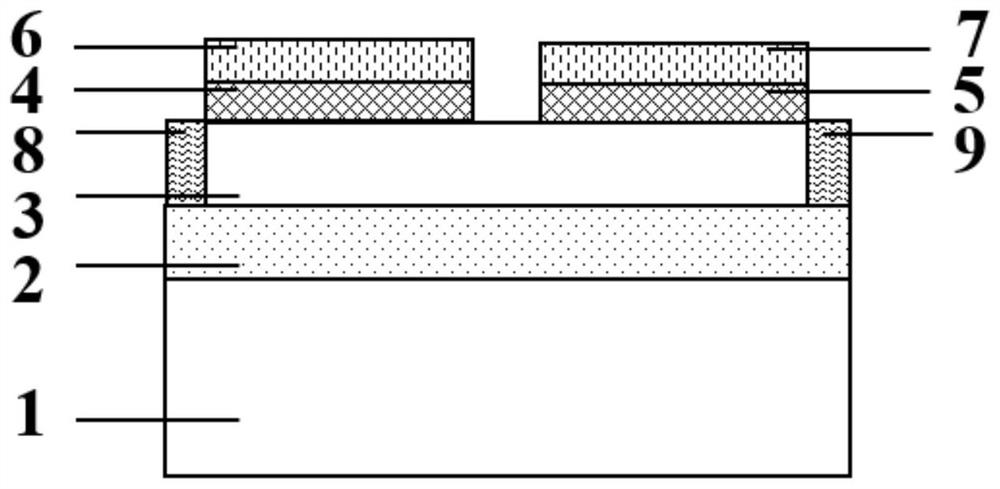
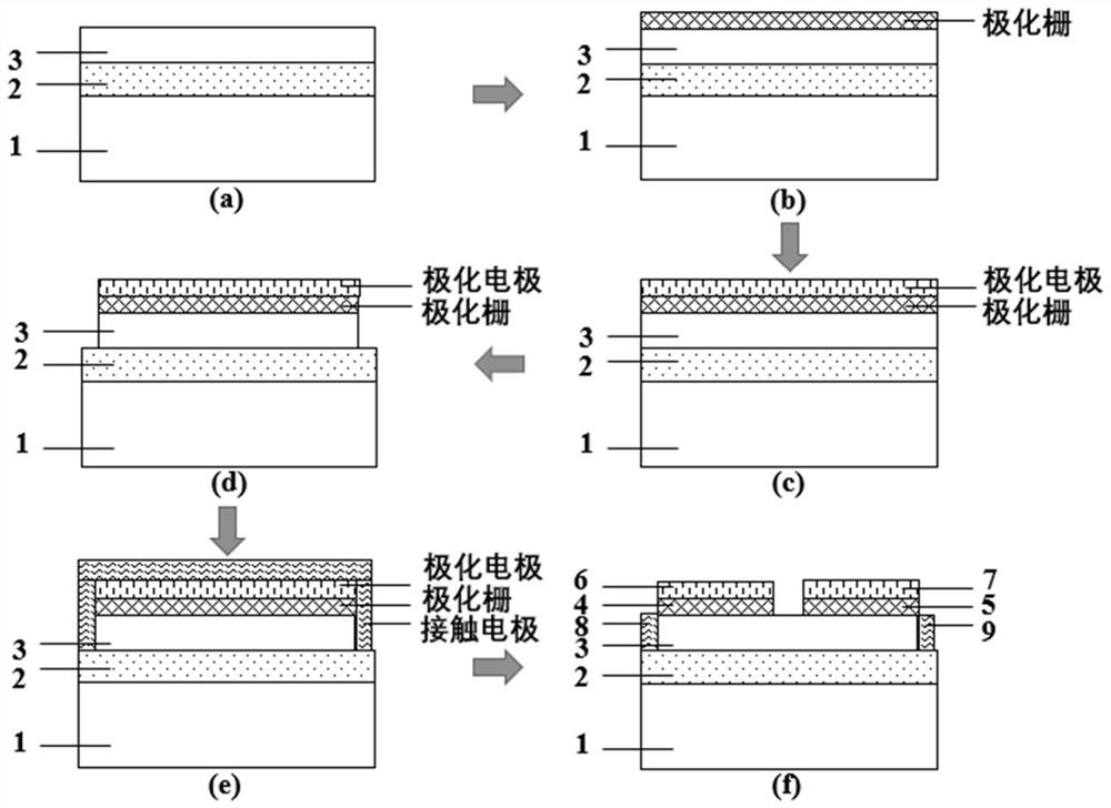
[0034] Select an SOI substrate composed of Si as the substrate 1, SiO2 as the insulating oxide layer 2, and Si as the channel layer 3, such as figure 2 (a).

[0035] Step 2: Deposit a ferroelectric layer.

[0036] Put the SOI substrate into the reaction chamber, use the atomic layer deposition process, use tetrakis (dimethylamino) zirconium as the precursor zirconium source, H2O or O3 as the precursor oxygen source, use N2 as the purge gas, and use 250°C as the reaction temperature, a 5nm thick ZrO2 ferroelectric layer is deposited on the surface of SOI as a polarization gate, such as figure 2 (b).

[0037] Step 3: Deposition of positive polarizing electrode layer.

[0038]Using the reactive sputtering process, the reaction chamber is first evacuated with a molecular pump and a cold pump until the vacuum pressure is 8E-6Torr, and then...

Embodiment 2

[0047] Embodiment 2: making based on HfO 2 Material-doped Ge channel PN junction memory device.

[0048] Step 1: Select the substrate.

[0049] Select a GOI substrate consisting of Ge as the substrate 1, borosilicate glass as the insulating oxide layer 2 and Ge as the channel layer 3, as figure 2 (a).

[0050] Step 2: depositing a ferroelectric layer.

[0051] Put the GOI substrate into the reaction chamber, use the atomic layer deposition process, with HfCl 4 As the precursor hafnium source, H2O or O3 is the precursor oxygen source, N2 is used as the purge gas, and the reaction temperature is 300 °C, and a 10nm thick HfO2 ferroelectric layer is deposited on the surface of GOI as a polarization gate, such as figure 2 (b).

[0052] Step 3: Depositing an active polarizing electrode layer.

[0053] 3.1) Using the reactive sputtering process, first use a molecular pump and a cold pump to evacuate the reaction chamber until the vacuum pressure is 8E-6Torr;

[0054] 3.2) Wi...

Embodiment 3

[0061] Embodiment 3: Fabricate a SiGe channel PN junction storage device based on HZO material doping.

[0062] Step A: Select the substrate.

[0063] Select a SiGeOI substrate composed of Si as the substrate 1, BPSG as the insulating oxide layer 2, and SiGe as the channel layer 3, such as figure 2 (a).

[0064] Step B: depositing a ferroelectric layer.

[0065] Put the SiGeOI substrate into the reaction chamber, use the atomic layer deposition process, use HfCl4 as the precursor hafnium source, use tetrakis(dimethylamino) zirconium as the precursor zirconium source, H2O or O3 as the precursor oxygen source, and N2 As a purge gas, a 15nm-thick HZO ferroelectric layer was deposited on the surface of SiGeOI as a polarization gate at 260°C as a reaction temperature, such as figure 2 (b).

[0066] Step C: depositing a positive polarizing electrode layer.

[0067] Using the reactive sputtering process, the reaction chamber is first evacuated with a molecular pump and a cold ...


PUM


Abstract

The invention discloses a PN junction memory device based on ferroelectric doping, and mainly aims to solve the problem that the existing PN junction memory device cannot realize switching of different conduction types. The device comprises a substrate (1), an insulating oxide layer (2) and a channel layer (3) from bottom to top, an anode (8) and a cathode (9) are arranged on two sides of the channel layer, an anode polarization grid (4) is arranged on the left of the upper portion of the channel layer, and a cathode polarization grid (5) is arranged on the right of the channel layer; an anode polarization electrode (6) and a cathode polarization electrode (7) are arranged on the upper portion of the anode polarization grid and the upper portion of the cathode polarization grid respectively, pulse voltages with different polarities are applied to the two polarization electrodes (6 and 7), and switching of PN junctions between different storage states is achieved by changing the application sequence of positive and negative pulses. According to the invention, the storage function of the PN junction memory device is expanded, the damage to the channel in the technological process is reduced, the power consumption is reduced, the on-state current and durability of the device are improved, and the method can be used for manufacturing a nonvolatile memory.

Description

technical field [0001] The invention belongs to the technical field of microelectronic devices, in particular to a manufacturing method of a PN junction storage device, which can be used for manufacturing nonvolatile memories. Background technique [0002] Memory is the memory used to store information in modern semiconductor technology. It is mainly used to store programs and various data, and can complete the reading and writing of programs or data at high speed. Volatile and non-volatile memory constitute the existing memory system, in which: non-volatile memory can repeatedly store, read, erase and other operations on data, and the stored data Long-term storage is still possible afterwards. Non-volatile storage combines the characteristics of non-volatility and low power consumption, and has very important applications in the field of data storage. However, frequent data transmission between different memories leads to the reduction of bandwidth and computing efficiency...

Claims


Application Information

Patent Timeline
IPC IPC(8): H01L45/00
CPCH10N70/20H10N70/841H10N70/881H10N70/011
Inventor 刘艳唐建周久人韩根全郝跃
Owner XIDIAN UNIV
Why Eureka
Try Eureka