
Hierarchical protection circuit for internal data of SoC

A technology for internal data and protection circuits, applied in the protection of internal/peripheral computer components, etc., can solve the problems of increasing SoC design complexity and design difficulties, and achieve the effect of low resource occupation and simple circuit

Pending Publication Date: 2021-07-23
10TH RES INST OF CETC
View PDF17 Cites 2 Cited by
  • Summary
  • Abstract
  • Description
  • Claims
  • Application Information

AI Technical Summary

Problems solved by technology

The scale of SoC chips is generally much larger than that of ordinary ASICs. At the same time, due to the design difficulties brought about by deep submicron technology, the complexity of SoC design is greatly increased.

Method used


Image

  • Hierarchical protection circuit for internal data of SoC
  • Hierarchical protection circuit for internal data of SoC

Examples


Embodiment Construction

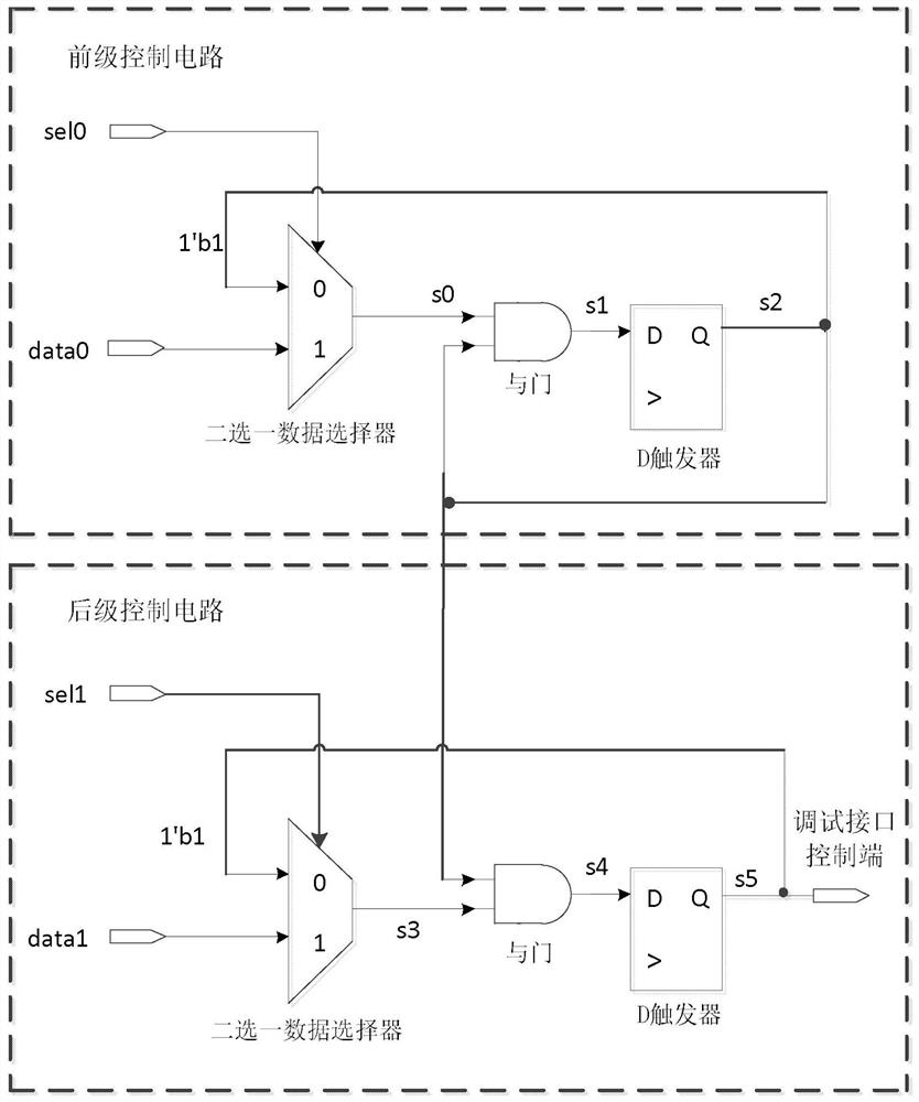
[0011] refer to figure 1 . In the preferred embodiment described below, based on the ARMv7 debugging architecture, a SoC chip internal data classification protection circuit includes a subsequent control circuit and a previous control circuit. The front-stage control circuit uses the input control signal and selection signal to generate an on-off signal, and the on-off signal directly acts on the rear-stage control circuit to control the output and on-off of the latter-stage circuit, and the on-off of the debugging interface of the latter-stage circuit; The front-stage D flip-flop of the control circuit is connected to the input end of the front-stage data selector (MUX) through the feedback line of the control terminal of the debugging interface. , output the value of the selected output result to the front-stage AND gate circuit VHD through the data output terminal, and add it to the previous-stage AND gate output terminal s1, turn on the D-side of the previous-stage D flip...


PUM


Abstract

The SoC chip internal data grading protection circuit disclosed by the invention is simple in circuit, low in resource consumption, safe and reliable. According to the technical scheme, a pre-stage control circuit generates an on-off signal by using an input control signal and a selection signal to control the output and on-off of a post-stage circuit; a D trigger of a pre-stage control circuit is connected with a data selector through a feedback line, the data selector selects one path of data as an input signal of an AND gate, a gating signal is sent to an AND gate circuit, the D trigger is conducted, a pulse triggering latch is used for realizing edge triggering of an output clock to a CLK-Q path delay signal s2, a first preceding-stage AND gate circuit parallel loop is connected with a second post-stage AND gate circuit to form a priority control circuit; and reading and writing of internal data of the SoC chip are controlled based on the ARMv7 debugging architecture. In a default state, the post-stage circuit performs immersion type or non-immersion type debugging on the external circuit; and the internal data of the SoC chip are protected in a grading manner.

Description

technical field [0001] The invention relates to a hierarchical protection circuit for internal data of a SoC chip based on an ARMv7 debugging architecture in the field of security chips. Background technique [0002] Security chips have greatly enhanced information security, and their applications are increasingly being integrated into national security and people's lives. With the continuous advancement of informatization, the means of attack on security chips are also increasing. But at the same time, attacks on security emerge in an endless stream, which makes it urgent to study the security protection of security chips. Nowadays, the attack technology specifically targeting chips has gone beyond dissection and reverse extraction, and has developed into deep-level simple power analysis SPA, differential power analysis DPA, fault analysis attacks, etc. Security SoC is the product of the combination of encryption technology and System on Chip (System on Chip) technology. ...

Claims


Application Information

Patent Timeline
IPC IPC(8): G06F21/72
CPCG06F21/72Y02D10/00
Inventor 徐波邓强许云龙王松明赵衡
Owner 10TH RES INST OF CETC
Learn More