Heterojunction material and application thereof

A heterojunction and molybdenum selenide technology, which is applied in sustainable manufacturing/processing, climate sustainability, semiconductor devices, etc., can solve the problems of limited performance and uncontrollable heterojunction preparation, and achieve large size and suppressed interface The effect of defect generation and broad application prospects

Active Publication Date: 2021-08-03
HUAZHONG UNIV OF SCI & TECH
View PDF11 Cites 0 Cited by
  • Summary
  • Abstract
  • Description
  • Claims
  • Application Information

AI Technical Summary

Problems solved by technology

[0006] The invention provides a heterojunction material and its application to solve the technical problems of uncontrollable preparation and limited performance of the existing heterojunction

Method used


Image

  • Heterojunction material and application thereof
  • Heterojunction material and application thereof
  • Heterojunction material and application thereof

Examples


Embodiment 1

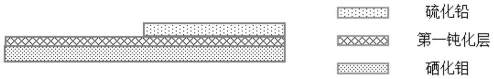
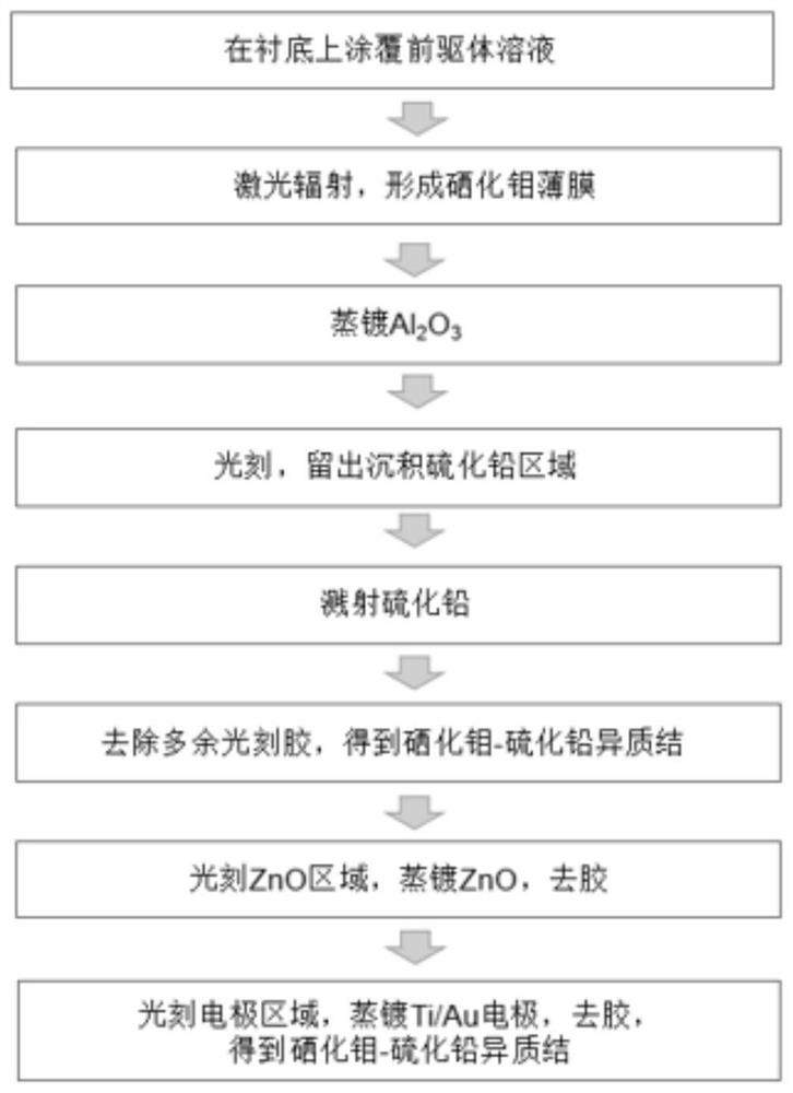
[0032] A heterojunction material such as figure 1 As shown, it includes: a molybdenum selenide film, a first passivation layer and a lead sulfide film stacked in sequence; wherein, the molybdenum selenide film is prepared by the following method: spin-coating the molybdenum selenide precursor solution onto the substrate, The precursor solution on the substrate is irradiated with a laser to obtain a molybdenum selenide thin film.

[0033] Lead sulfide is an important semiconductor material with a narrow band gap (0.41eV) and a large Bohr radius (18nm) because of its large dielectric constant and high refractive index. This material is widely used in national defense, industrial and agricultural construction. In recent decades, it has received extensive attention from the scientific community. Molybdenum selenide is a transition metal sulfide material with a layered structure. It has a typical layered structure. Because of its strong light absorption and high photoelectric conv...

Embodiment 2

[0039] An application of the above-mentioned heterojunction material to a semiconductor device.

[0040] Large-scale, high-quality heterojunctions can be grown on specific substrates to meet the application requirements of industrial production. The heterojunction prepared by molybdenum selenide and lead sulfide has the characteristics of wide spectral response range and high light absorption intensity, which is conducive to the preparation of high-efficiency optoelectronic devices. Preferably, the semiconductor device is a photodetector.

Embodiment 3

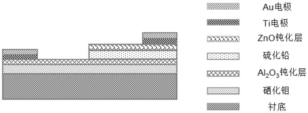
[0042] A photodetector, such as figure 2 As shown, it includes: an insulating substrate, the heterojunction material as described in Embodiment 1 above, a second passivation layer and two electrodes. The molybdenum selenide film in the heterojunction material is stacked on the upper surface of the insulating substrate; the second passivation layer is on the upper surface of the molybdenum selenide film; two electrodes are respectively on the upper surface of the first passivation layer and the second passivation layer surface.


PUM

PropertyMeasurementUnit
lengthaaaaaaaaaa
widthaaaaaaaaaa
thicknessaaaaaaaaaa

Abstract

The invention belongs to the technical field of semiconductor device preparation, and particularly relates to a heterojunction material and application thereof, and the heterojunction material comprises a molybdenum selenide thin film, a first passivation layer and a lead sulfide thin film which are sequentially stacked, wherein the molybdenum selenide thin film is prepared through laser radiation. The heterojunction material can be applied to a photoelectric detector and structurally comprises an insulating substrate, the heterojunction material, a passivation layer and an electrode. The molybdenum selenide thin film is prepared through laser radiation, the lead sulfide thin film is prepared through magnetron sputtering, and the heterojunction area is prepared through photoetching selection. The photoelectric detector can detect infrared light and near-infrared light and is short in response time and high in light responsivity, and the preparation method has the advantages of simple and convenient process, low cost and large-scale production, so that the heterojunction photoelectric detector has a very good application prospect.

Description

technical field [0001] The invention belongs to the technical field of semiconductor device preparation, and more specifically relates to a heterojunction material and its application. Background technique [0002] Semiconductor photodetectors are devices that use the photoelectric effect in semiconductor materials to receive and detect optical signals, and are an indispensable part of modern optoelectronic devices. However, existing photodetectors have problems such as low photoelectric conversion efficiency, slow response time, and limited detection band. Therefore, it is urgent to study a high-performance infrared photodetector with wide-band response. [0003] Two-dimensional material heterojunction refers to a composite structure composed of two or more different two-dimensional materials in close contact. It has excellent characteristics of different materials and can exhibit performance different from that of a single material. Therefore, heterojunction is the main bo...

Claims


Application Information

Patent Timeline
Patent Type & Authority Applications(China)
IPC IPC(8): H01L31/032H01L31/0216H01L31/102H01L31/18
CPCH01L31/032H01L31/0324H01L31/02161H01L31/18H01L31/102Y02P70/50
Inventor 曾祥斌王曦雅胡一说王文照陆晶晶王君豪肖永红周宇飞王士博陈铎张茂发
Owner HUAZHONG UNIV OF SCI & TECH
Why Eureka
Try Eureka