
FD-SOI back deep channel isolation process based on bonding process

A technology of FD-SOI and bonding process, which is applied to semiconductor devices, electrical components, circuits, etc., and can solve the problems of large chip area and high cost of FDSOI transistors

Active Publication Date: 2021-08-20
GUANGDONG GREATER BAY AREA INST OF INTEGRATED CIRCUIT & SYST +1
View PDF4 Cites 0 Cited by
  • Summary
  • Abstract
  • Description
  • Claims
  • Application Information

AI Technical Summary

Problems solved by technology

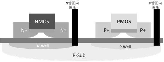
However if figure 1 As shown, the back bias voltage control terminal of the FDSOI transistor on the existing wafer is drawn from the wafer, and competes with the gate, source and drain for the metal interconnection area, and this structure often leads to a decrease in the chip area of ​​the FDSOI transistor. Larger than conventional bulk silicon or FinFET
[0004] In addition, in the manufacturing process of FDSOI-based chips, isolation trenches are first made on the wafer, then FDSOI transistors are made on the wafer, and finally back-bias via holes are made on the FDSOI transistors. According to the existing manufacturing process , when making isolation trenches, FDSOI transistors, and back-bias vias on the wafer, a photomask is required, which is costly, and further optimization of the chip manufacturing process is required to reduce manufacturing costs

Method used


Image

  • FD-SOI back deep channel isolation process based on bonding process
  • FD-SOI back deep channel isolation process based on bonding process
  • FD-SOI back deep channel isolation process based on bonding process

Examples


Embodiment Construction

[0038] The present invention is described in further detail now in conjunction with accompanying drawing. These drawings are all simplified schematic diagrams, which only illustrate the basic structure of the present invention in a schematic manner, so they only show the configurations related to the present invention.

[0039] Such as Figure 4 As shown, a bonding process-based FD-SOI rear deep trench isolation process includes the following steps:

[0040] S1: Make the first chip 101 on the first wafer 100, make M first bonding Pad103 on the metal wiring layer 102 of the uppermost layer of the first chip 101, M is a positive integer, and the tungsten on the first chip 101 Make contact Pad104 in the through hole layer;

[0041] The schematic diagram of the structure after the first chip 101, the first bonded Pad103 and the contact Pad104 are fabricated on the first wafer 100 can be referred to Figure 5 , Figure 5 The second chip 101, the first bonding Pad103 and the con...


PUM


Abstract

The invention relates to the technical field of semiconductors, and discloses an FD-SOI back deep channel isolation process based on a bonding process. M first bonding pads are manufactured on a metal wiring layer on the uppermost layer of a first chip, M second bonding pads are manufactured on a metal wiring layer on the uppermost layer of a second chip, and then the first chip and the second chip are aligned and bound, so that the M first bonding Pads on the first chip are electrically connected with the M second bonding Pads on the second chip in a one-to-one manner. The area required for integrating the first chip and the second chip can be reduced, in addition, isolation grooves in the first chip and isolation grooves in the second chip are arranged up and down, the proportion of the isolation grooves in the whole chip area is reduced, and the chip area can be reduced; and finally, deep channel isolation is manufactured while the through hole layer of the second chip is manufactured, so that the manufacturing cost and period of the chip are greatly reduced, and the isolation effect of a chip device is enhanced by evolving shallow channel isolation to deep channel isolation.

Description

technical field [0001] The invention relates to the technical field of semiconductors, in particular to a back deep trench isolation process of FD-SOI based on a bonding process. Background technique [0002] At present, in the chip manufacturing process, most of the different circuit modules on the chip are manufactured on different wafers according to the process technology, and then these circuit modules are tiled and integrated on the same base plate to realize the electrical properties of these circuit modules. connection, and finally package the bottom plate to form the final product. For example, it integrates the central processing unit CPU, random access memory RAM, read-only memory ROM, various I / O ports and interrupt systems, and timer / counter single-chip microcomputer chips. However, as the functions of the chip continue to increase, there are more and more circuit modules in the chip. If the circuit modules are still tiled on the bottom plate, the area of ​​the...

Claims


Application Information

Patent Timeline
IPC IPC(8): H01L21/762H01L21/768H01L21/027H01L21/50H01L21/60H01L25/07
CPCH01L21/027H01L21/50H01L21/76224H01L21/76877H01L21/76898H01L24/06H01L24/80H01L25/071
Inventor 高峰叶甜春罗军赵杰薛静
Owner GUANGDONG GREATER BAY AREA INST OF INTEGRATED CIRCUIT & SYST
Learn More