Thin film preparation method, high-throughput combined material chip preparation method and system thereof

A technology for the preparation of composite material chips and thin films, which can be used in metal material coating processes, semiconductor/solid-state device manufacturing, ion implantation and plating, etc., and can solve problems such as time-consuming and labor-intensive

Active Publication Date: 2021-09-03
UNIV OF ELECTRONIC SCI & TECH OF CHINA
View PDF18 Cites 0 Cited by
  • Summary
  • Abstract
  • Description
  • Claims
  • Application Information

AI Technical Summary

Problems solved by technology

[0004]In order to overcome the existing high-throughput thin film sample technology based on the multilayer film diffusion process, material sample preparation needs to match special heat treatment temperature, atmosphere and preparation process, which is time-consuming To solve technical problems such as laboriousness, the present invention provides a thin film preparation method, a high-throughput composite material chip preparation method and a device thereof

Method used


Image

  • Thin film preparation method, high-throughput combined material chip preparation method and system thereof
  • Thin film preparation method, high-throughput combined material chip preparation method and system thereof
  • Thin film preparation method, high-throughput combined material chip preparation method and system thereof

Examples


Embodiment Construction

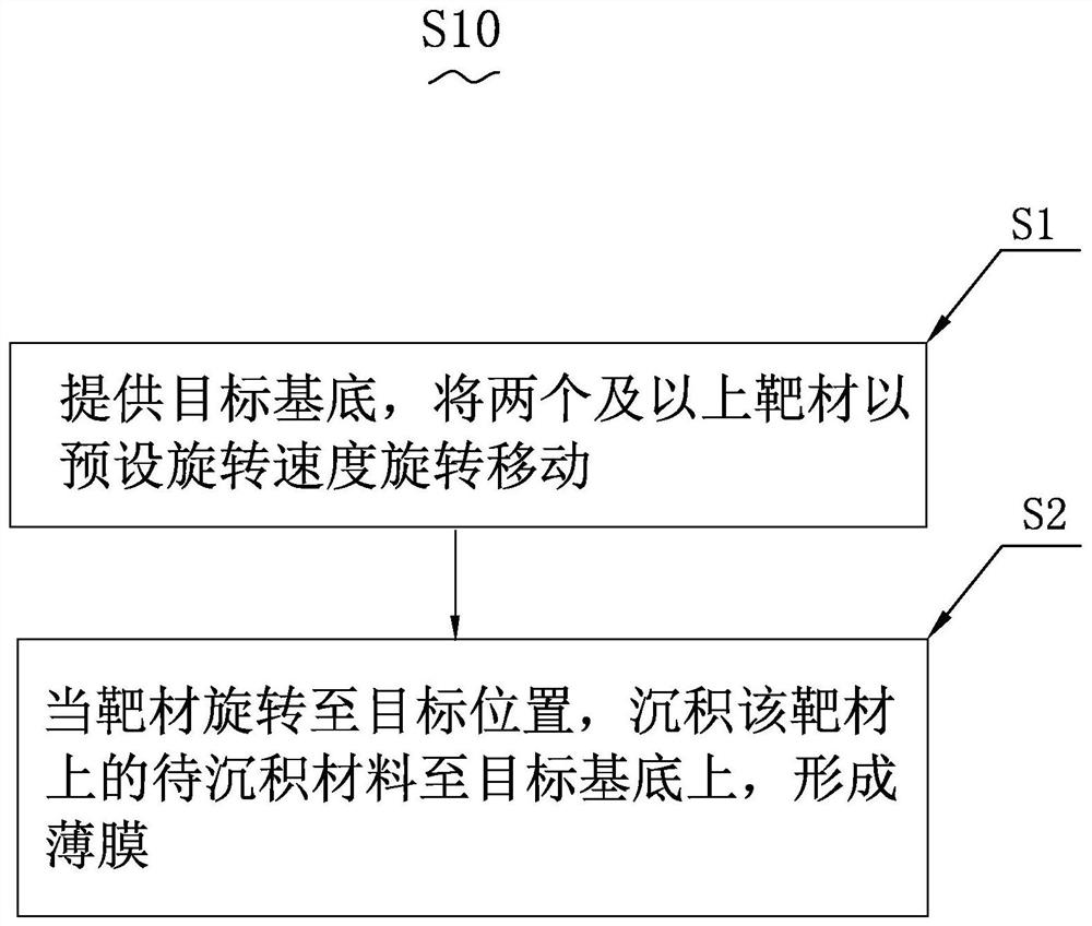
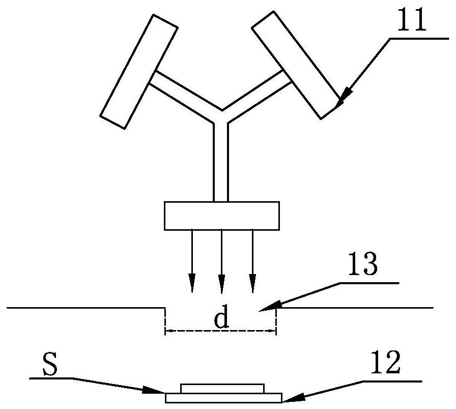
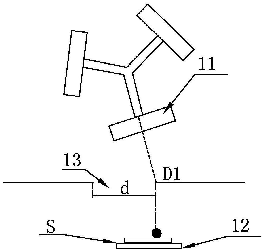
[0047] In order to make the purpose, technical solutions and advantages of the present invention more clear, the present invention will be further described in detail below in conjunction with the accompanying drawings and implementation examples. It should be understood that the specific embodiments described here are only used to explain the present invention, not to limit the present invention.

[0048] "One embodiment", "preferred embodiment", "embodiment" or "multiple embodiments" mentioned in this specification means that the specific features, structures, characteristics or functions described in conjunction with the embodiments are included in the present invention In at least one embodiment and may be in more than one embodiment. The appearances of the phrases "in one embodiment," "in an embodiment," or "in multiple embodiments" in various places in this specification are not necessarily all referring to the same embodiment or the same multiple embodiments.

[0049] ...


PUM


Abstract

The invention relates to the field of thin film material preparation, and provides a thin film preparation method which can be used for rotating a target material and controlling the rotating speed of the target material, so that when a to-be-deposited material of a previous target material does not form a layered thin film in an island-shaped growth state, another target material continues to be deposited, the to-be-deposited materials of different target materials can be deposited in an atom mixing manner, so that uniform mixing of various materials can be realized without additionally arranging a heat treatment process, the thin film preparation difficulty is greatly reduced, and the precision and yield of thin film preparation are improved. The invention further provides a preparation method and system for a high-throughput combined material chip, high-throughput combined deposition of the to-be-deposited materials of different target materials in an atom mixing mode can be achieved, the preparation process of the high-throughput combined material chip is simplified, the high-throughput combined material chip is obtained by combining the related high-throughput characterization technology, mass material data is rapidly provided for construction of a material gene database, and finally on-demand design and intelligent manufacturing of materials are promoted.

Description

【Technical field】 [0001] The invention relates to the field of thin film material preparation, in particular to a thin film preparation method, a high-throughput combined material chip preparation method and a device thereof. 【Background technique】 [0002] With the continuous deepening of material technology research, high-throughput material test technology has been developed rapidly, which is essentially the controllable distribution of multiple components or preparation processes on a substrate through microelectronics technology or other precision preparation methods and precise micro-area preparation, realize the preparation of up to 1 million sample units with different components or other process parameters on a substrate, and cooperate with high-throughput fast scanning or parallel characterization technology, it is possible to realize a complex system in a relatively short period of time. The systematic preparation and testing of experimental samples, the final qua...

Claims


Application Information

Patent Timeline
IPC IPC(8): C23C14/34C23C14/54C23C14/04H01L21/285
CPCC23C14/3464C23C14/542C23C14/548C23C14/042H01L21/2855
Inventor 闫宗楷刘奕向勇徐子明贾春阳
Owner UNIV OF ELECTRONIC SCI & TECH OF CHINA
Why Eureka
Try Eureka