Preparation method of silicon nanostructure and laser

A silicon nanotechnology, laser technology, applied in lasers, laser parts, nanotechnology and other directions, can solve the problem of the quality of silicon needs to be improved

Inactive Publication Date: 2021-09-07
INST OF MICROELECTRONICS CHINESE ACAD OF SCI
View PDF6 Cites 2 Cited by
  • Summary
  • Abstract
  • Description
  • Claims
  • Application Information

AI Technical Summary

Problems solved by technology

[0003] At present, there are mainly two methods for making nano-sized silicon structures. One is bottom-up, that is, using silicon epitaxial growth technology to grow a silicon structure that meets the requirements on a substrate with a photoresist as a mask. The quality of silicon grown by this technology needs to be improved; the second is the more commonly used silicon etching technology using a mask. The key to this technology is to manufacture a mask that meets the requirements of nanometer size.

Method used


Image

  • Preparation method of silicon nanostructure and laser
  • Preparation method of silicon nanostructure and laser
  • Preparation method of silicon nanostructure and laser

Examples


preparation example Construction

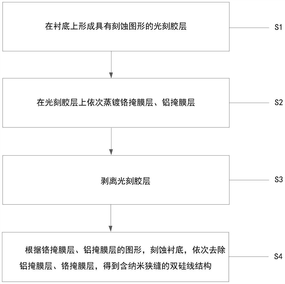
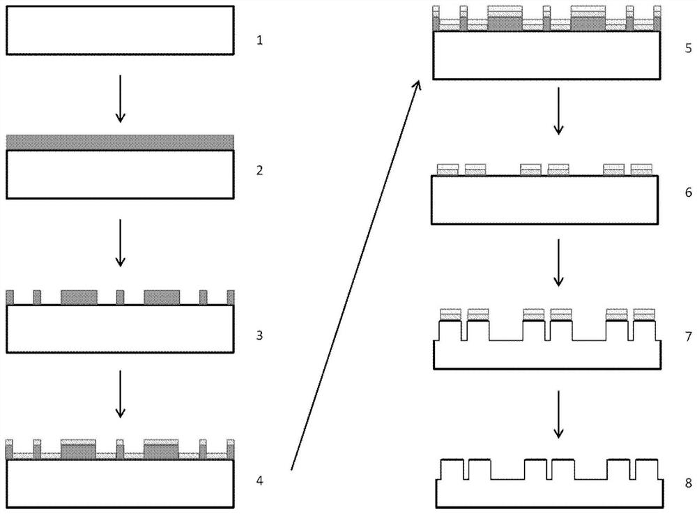
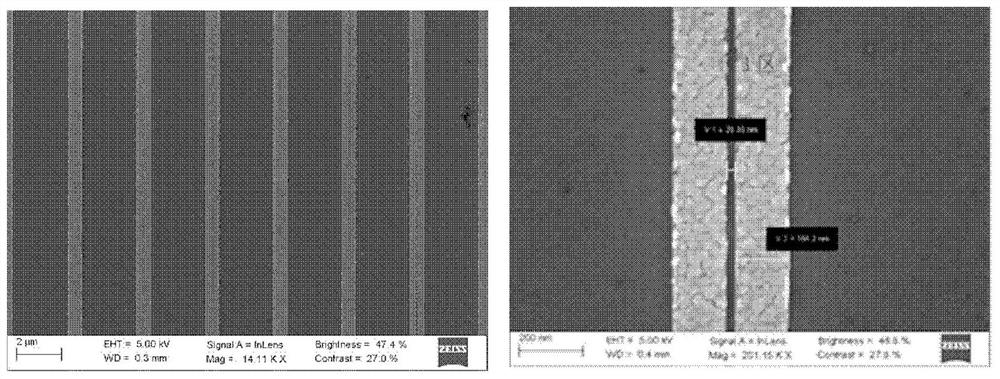
[0051] figure 2 Schematically showing a structural diagram of a method for preparing a silicon nanostructure according to an embodiment of the present disclosure, which completely includes the following steps:

[0052] Step 1, providing an SOI sheet substrate;

[0053] Step 2. Carry out electron beam lithography on the SOI sheet substrate. The selected photoresist is PMMA A2 electron beam glue. Before coating, bake the SOI sheet at 150° for 2 minutes to dry the surface moisture of the SOI sheet. During spin coating, 4000 Turn and bake at 180° for 2 minutes to form an electron beam photoresist film of about 70nm;

[0054] Step 3, forming a pattern by electron beam lithography, which is equivalent to step S1;

[0055] Step 4, electron beam evaporation, evaporation metal mask Cr, its thickness is 5nm;

[0056] Step 5, electron beam evaporation, evaporating metal mask Al, the thickness of which is 15nm, which is equivalent to step S2;

[0057] Step 6, peel off the photoresist...


PUM

PropertyMeasurementUnit
thicknessaaaaaaaaaa
thicknessaaaaaaaaaa
heightaaaaaaaaaa

Abstract

The invention provides a preparation method of a silicon nanostructure and a laser. The preparation method comprises the following steps: forming a photoresist layer with an etched pattern on a substrate; sequentially evaporating a chromium mask layer and an aluminum mask layer on the photoresist layer; stripping the photoresist layer; and etching the substrate according to the patterns of the chromium mask layer and the aluminum mask layer, and sequentially removing the aluminum mask layer and the chromium mask layer to obtain the double-silicon-line structure containing the nano slit. According to the preparation method, the double-silicon-line structure containing the nano slit can be prepared, the manufacturing process is simple, when the outer layer is coated with the thin film containing the gain material, the optical characteristic of the structure shows the performance of laser, and the structure can be used for a nano laser. The invention further provides a laser with the double-silicon-line structure.

Description

technical field [0001] The disclosure relates to the technical field of nanostructure preparation, in particular to a method for preparing a silicon nanostructure and a laser. Background technique [0002] With the development of microelectronics technology and the further expansion of Moore's Law, devices are developing towards miniaturization and miniaturization. The miniaturization of devices largely depends on the continuous development of micro-nano processing technology. For various bulk silicon MEMS devices, the widespread adoption and development of silicon dry etching technology is crucial to the miniaturization of devices, including high aspect ratio dry etching technology, nanoscale etching technology, etc. Nano-scale etching technology is a key processing step of nano-devices, and its related nano-scale mask processing and stripping technology directly determines the nano-size of the device to be processed. [0003] At present, there are mainly two methods for m...

Claims


Application Information

Patent Timeline
Patent Type & Authority Applications(China)
IPC IPC(8): H01L21/308H01S3/06B82Y40/00
CPCH01L21/3081H01S3/0627B82Y40/00
Inventor 陈生琼史丽娜牛洁斌李龙杰尚潇谢常青
Owner INST OF MICROELECTRONICS CHINESE ACAD OF SCI
Why Eureka
Try Eureka