High-performance single-photon pixel spad structure

A single-photon, high-performance technology, applied in electrical components, diodes, electro-solid devices, etc., to solve problems such as large pixel size, limited application, and difficult SPAD compatibility

Pending Publication Date: 2021-09-10
上海矽印科技有限公司
View PDF0 Cites 3 Cited by
  • Summary
  • Abstract
  • Description
  • Claims
  • Application Information

AI Technical Summary

Problems solved by technology

In the commonly used SPAD structure, the reverse bias voltage is above 15V, which makes it difficult for SPAD to be compatible with standard CMOS circuits. At the same time, high voltage requires strong isolation means, which leads to a huge single pixel size, which cannot improve the spatial resolution of detection. Seriously limit its application in tiny devices such as mobile phones

Method used


Image

  • High-performance single-photon pixel spad structure
  • High-performance single-photon pixel spad structure
  • High-performance single-photon pixel spad structure

Examples


specific Embodiment 1

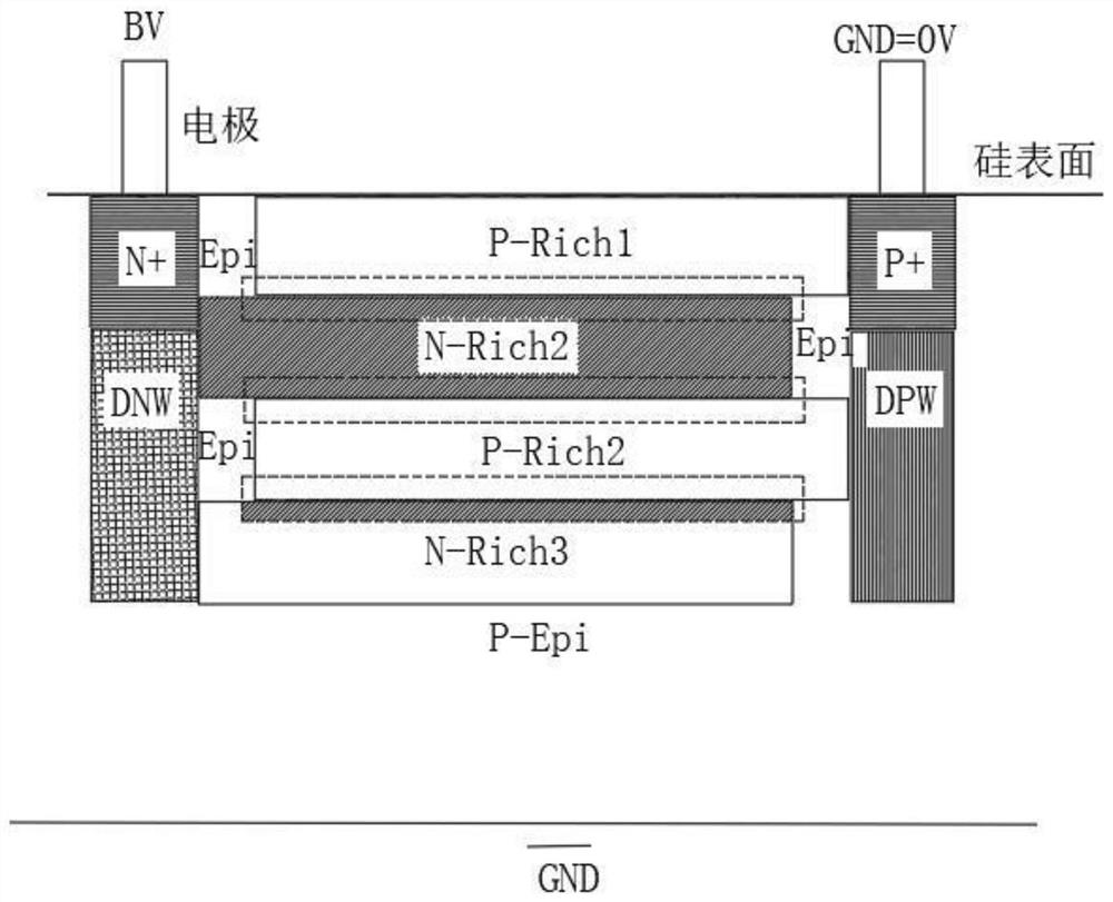
[0035] Such as figure 1 As shown, in the actual process, the silicon surface is directly in contact with silicon dioxide, which leads to the mismatch of the covalent bonds of the silicon atoms on the surface, thus generating a large amount of dark current, which makes the SPAD prone to breakdown even in the absence of light. , that is, the dark count rate is very high. This example adopts a surface P-type doped structure; this structure forms a P-N-P-N type space doping structure. Since the silicon surface is filled with P-type doping, the broken dangling bonds of silicon are replaced by P-type Impurities are trapped, thereby reducing dark current.

specific Embodiment 2

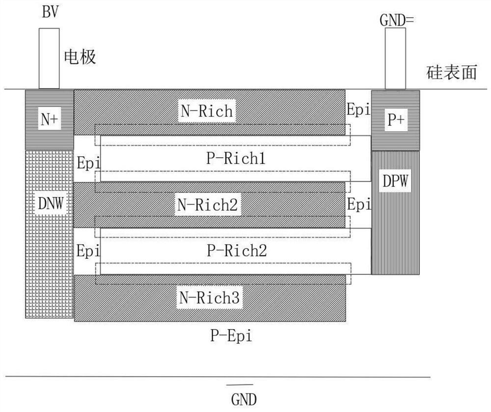
[0037] Such as figure 2 As shown, in the above application, P-EPI is used for isolation. Low-concentration doped PN structure isolation makes the width of the depletion region wider, which is not conducive to reducing the size of SPAD. In this example, N-type impurities and P-type impurities are used for isolation. Among them, the doping concentration of N-type impurities is lower than that of N-rich, and the doping of P-type impurities is lower than that of P-rich. The concentrations of N-type impurities and P-type impurities are higher than the concentration of P-type epitaxial layer p-epid At the same time, the silicon surface is separated by STI by digging grooves; wherein, in this specific embodiment, N-type adopts phosphorus, P-type adopts boron implantation, the first layer of N-type impurity implantation layer N-rich1, and the second layer of N-type impurity implantation layer The energies of N-rich2 and the third N-type impurity implanted layer N-rich3 are: 40KeV, 17...


PUM


Abstract

The invention discloses a high-performance single-photon pixel spad structure, and relates to the technical field of integrated circuits. The device comprises a silicon surface, a cathode and an anode, high voltage is applied to the cathode, and the anode is grounded; impurities with different properties are doped on the surface of silicon for multiple times, ions of N-type impurities and P-type impurities are injected with energy to form a plurality of back-to-back PN junctions, and finally the plurality of back-to-back PN junctions are connected in parallel; multiple times of doping are adopted, so that signals can be effectively led out from the deep part, and any two PN junctions are connected in parallel, so that the depth of a space depletion region is effectively increased in the longitudinal direction; the cathode and the deep N well injection are isolated from the P-type impurities by using epitaxial layer low-concentration doping; and the anode and the deep P well injection are isolated from the N-type impurities by using epitaxial layer low-concentration doping. According to the invention, the depth of the depletion region is effectively expanded, the detection efficiency is improved, and the diffusion time of photoelectrons is reduced, so that the time jitter is reduced, and the SPAD avalanche voltage can be effectively reduced.

Description

technical field [0001] The invention belongs to the technical field of integrated circuits, in particular to a high-performance single-photon pixel spad structure. Background technique [0002] The SPAD physical structure is a reverse PN junction. In the working state, it applies a high reverse bias voltage across the cathode N and the anode P, so that the diode works in Geiger mode. When photons are absorbed in its depletion region, the carrier multiplication effect occurs due to the high electric field strength, which instantly reduces the reverse resistance of the PN junction and generates a high reverse current. In the commonly used SPAD structure, the reverse bias voltage is above 15V, which makes it difficult for SPAD to be compatible with standard CMOS circuits. At the same time, high voltage requires strong isolation means, which leads to a huge single pixel size, which cannot improve the spatial resolution of detection. Seriously limit its application in tiny devic...

Claims


Application Information

Patent Timeline
Patent Type & Authority Applications(China)
IPC IPC(8): H01L31/0352H01L31/107H01L27/146
CPCH01L31/035272H01L31/107H01L27/14605H01L27/14643
Inventor 武大猷江建明张睿轶李高志
Owner 上海矽印科技有限公司
Why Eureka
Try Eureka