Silicon carbide crystal, seed crystal used by silicon carbide crystal and preparation method of seed crystal
A technology of silicon carbide seeds and silicon carbide single crystals, which is applied in chemical instruments and methods, crystal growth, and from chemically reactive gases, etc., can solve the problem of difficulty in obtaining high-quality seed wafers, long cycle times, and difficulty in ensuring silicon carbide crystals Quality and other issues
- Summary
- Abstract
- Description
- Claims
- Application Information
AI Technical Summary
Problems solved by technology
Method used
Image


Examples
Embodiment 1
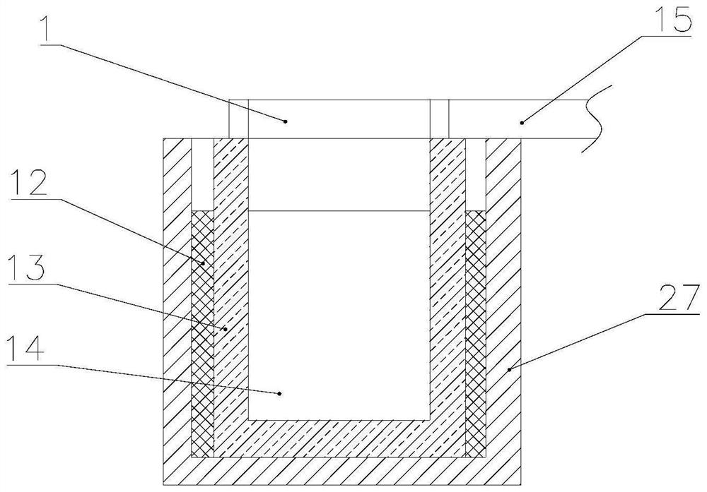
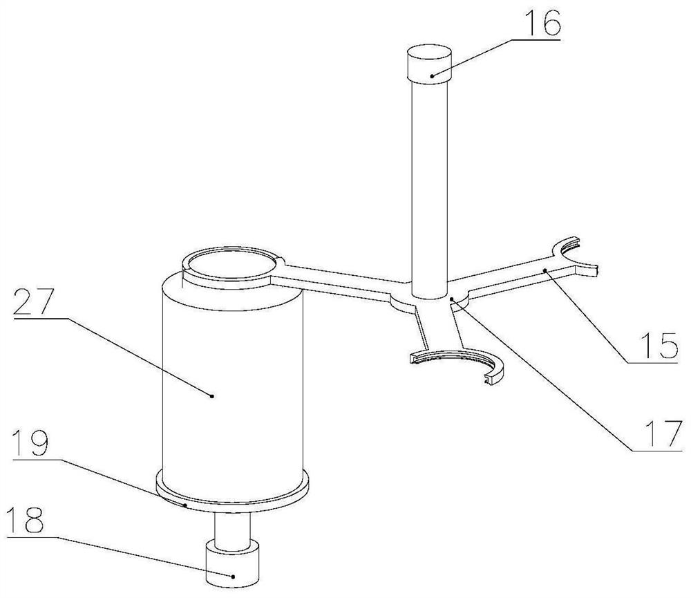
[0086] refer to figure 1 , the present embodiment provides a preparation device for improving the quality of seed crystals, which includes: a processing chamber 11, a heating unit 12 and a loading unit; wherein, a crucible 13 is provided in the processing chamber 11, and the crucible 13 is used to hold raw materials The heating unit 12 is arranged on the periphery of the crucible 13, and is used to melt the raw material into a molten state component 14 and sublimate to the seed crystal 1, so as to repair or reconstruct the atomic steps of the seed crystal growth surface; the upper edge of the heating unit 12 does not exceed the melting The liquid level of the component 14 in the molten state; By arranging the upper edge of the heating unit 12 not to exceed the liquid level of the molten component 14, it is avoided that the heating unit 12 heats the area between the liquid level of the molten component 14 and the seed crystal 1, thereby ensuring the liquid level of the molten c...
Embodiment 2
[0133] The preparation of embodiment 2 seed crystals
[0134] refer to Figure 1~3 According to an embodiment of the present application, a method for preparing a seed crystal 1 using the device of Example 1 includes the following steps:
[0135] 1) Loading: fix the seed crystal to be processed above the crucible, fill the crucible with raw materials, and place the seed crystal 1 and the crucible in the crystal processing chamber;
[0136] 2) Impurity removal: pump the pressure in the crystal processing chamber to 10 -6 Below mbar, pass inert gas to 300~500mbar, repeat this process at least twice;
[0137] 3) Preheating the seed crystal: pump the pressure in the crystal processing chamber to 10 -6 Below mbar, heat the raw materials in the crucible to melt the raw materials to form molten components, adjust the distance between the growth surface of the seed crystal and the liquid surface of the molten components to 10-100 mm, and preheat for 30-120 minutes;
[0138] 4) Ste...
Embodiment 3
[0146] The characterization of embodiment 3 seed crystal
[0147] The seed crystal prepared in Example 2 was characterized, and its scratch condition, step state, doping element doping concentration, TTV value, BOW value, Warp value and defect density were tested. The test results are shown in Table 2, wherein the doping The elements are reactive elements other than carbon and silicon.
[0148] Table 2
[0149]
[0150]
[0151]
[0152] It can be seen from the above table that through the adjustment and combination of various conditions in this embodiment, the repair and reconstruction of the atomic steps on the growth surface of the silicon carbide seed crystal can be realized, and the state of the steps can be freely controlled; in addition, the surface of the seed crystal can also be controlled The scratch has a slight repairing effect; therefore, compared with the traditional seed crystal, the step information of the seed crystal of the present application is comp...
PUM
 Abstract
Description
Claims
Application Information
 - R&D Engineer
- R&D Manager
- IP Professional
- Industry Leading Data Capabilities
- Powerful AI technology
- Patent DNA Extraction
Browse by: Latest US Patents, China's latest patents, Technical Efficacy Thesaurus, Application Domain, Technology Topic.
© 2024 PatSnap. All rights reserved.Legal|Privacy policy|Modern Slavery Act Transparency Statement|Sitemap