GaN-based HEMT device based on substrate conductive hole and preparation method of GaN-based HEMT device

A conductive hole and substrate technology, which is applied in the field of GaN-based HEMT devices based on substrate conductive holes and its preparation, can solve the problems of high manufacturing and equipment costs and lower yields

Pending Publication Date: 2021-09-14
上海新微半导体有限公司
View PDF3 Cites 4 Cited by
  • Summary
  • Abstract
  • Description
  • Claims
  • Application Information

AI Technical Summary

Problems solved by technology

[0004] In view of the shortcomings of the prior art described above, the purpose of the present invention is to provide a GaN-based HEMT device based on substrate conductive holes and its preparation method, which is used to solve the problem of the GaN-based HEMT device in the prior art when the source metal is drawn out. The cost of preparation and equipment is high and it is easy to lead to the problem of lower yield

Method used


Image

  • GaN-based HEMT device based on substrate conductive hole and preparation method of GaN-based HEMT device
  • GaN-based HEMT device based on substrate conductive hole and preparation method of GaN-based HEMT device
  • GaN-based HEMT device based on substrate conductive hole and preparation method of GaN-based HEMT device

Examples


Embodiment 1

[0055] Such as Figure 1 to Figure 10 As shown, this embodiment provides a method for preparing a GaN-based HEMT device based on substrate conductive holes. The device may be a radio frequency device, for example. The preparation method includes the steps of:

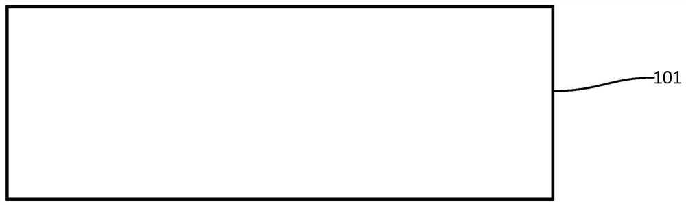
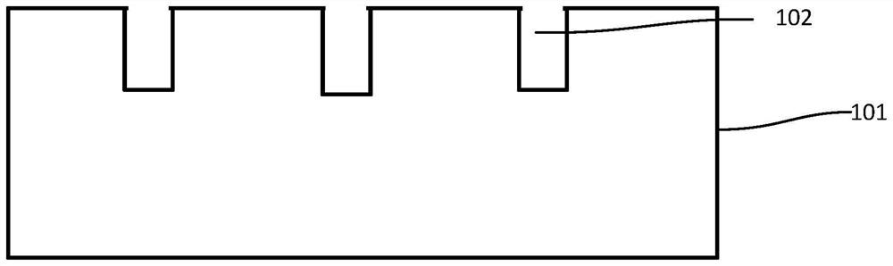
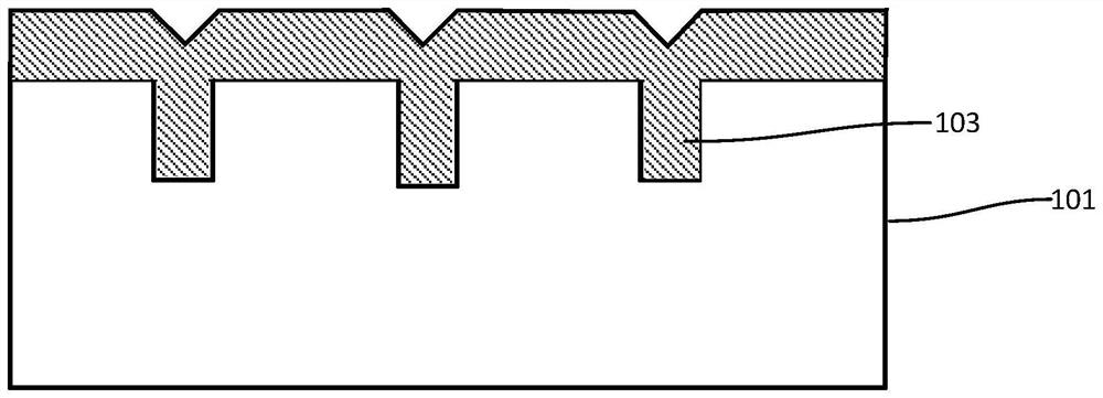
[0056] Such as Figure 1 ~ Figure 2 As shown, step 1) is first performed to provide a substrate 101, the substrate 101 includes a first main surface and a second main surface opposite, and a deep groove is etched in the first main surface of the substrate 101 Groove 102, the deep trench 102 is set corresponding to the source of the GaN-based HEMT device.

[0057] As an example, the substrate 101 includes one of a silicon-based substrate, a silicon carbide substrate, a gallium nitride substrate, a sapphire substrate, and a diamond substrate. In this embodiment, the substrate 101 is selected as a semi-insulating silicon substrate, which is used as the substrate required for the growth of the epitaxial layer structure of ...

Embodiment 2

[0078] Such as Figure 11 As shown, this embodiment provides a GaN-based HEMT device and its preparation method, the basic steps and basic structure of which are as in Embodiment 1, wherein the difference from Embodiment 1 lies in: the sidewall of the deep trench and the A diffusion barrier layer 201 is also formed between the conductive material layers, and the diffusion barrier layer 201 includes SiO 2 , SiN, Al 2 o 3 , AlN, HfO 2 A stacked structure of one or more of them is used to prevent dopant elements in the conductive silicon layer from diffusing into the substrate, so as to improve the electrical stability of the device.

Embodiment 3

[0080] Such as Figure 12 As shown, this embodiment provides a GaN-based HEMT device and its preparation method, its basic steps and basic structure are as in Embodiment 1, wherein, the difference from Embodiment 1 lies in that each source metal is connected to a corresponding source There are multiple ultra-deep holes 110 and connection layers 111 to reduce the width of the source deep holes, so that the connection layer 111, such as a conductive silicon layer, can more easily fill the source deep holes 110, improving the efficiency and process stability of the manufacturing process.


PUM


Abstract

The invention provides a GaN-based HEMT device based on a substrate conductive hole and a preparation method of the GaN-based HEMT device. According to the method, a deep groove is formed in a substrate, and filled with a conductive material layer to form a conductive hole, and a source deep hole is prepared in an epitaxial layer structure, so that a source metal is connected to the conductive hole; after the front surface structure of the GaN-based HEMT device is manufactured, thinning is carried out to expose the conductive hole from the back surface of the substrate; and therefore, back etching of the substrate in the later period is avoided, damage of etching to the front surface structure of the device is avoided, the yield of the device is effectively improved, and production equipment and cost are saved. After the preparation of the front surface structure of the device is completed, complicated deep etching, electroplating and other process steps are not needed any more, so that the influence of the subsequent process on the reliability of the device can be reduced.

Description

technical field [0001] The invention belongs to the field of semiconductor design and manufacture, in particular to a GaN-based HEMT device based on substrate conductive holes and a preparation method thereof. Background technique [0002] With the advent of the 5G era, the demand for high-frequency and high-power radio frequency devices in the communication field is becoming stronger and stronger. Due to its unique material properties, GaN materials are expected to be used in the future communication field. Due to the difficulty in manufacturing GaN substrates, GaN materials are generally formed by epitaxial growth on Si / SiC substrates. The top of the epitaxial structure can be changed by doping Al or In composition during epitaxial growth to form a high electron mobility The two-dimensional electron gas structure, based on this structure to manufacture GaN-based HEMT devices. [0003] The source of a GaN-based HEMT RF device usually needs to be connected to the back of th...

Claims


Application Information

Patent Timeline
Patent Type & Authority Applications(China)
IPC IPC(8): H01L29/778H01L29/06H01L21/335
CPCH01L29/7786H01L29/0603H01L29/0684H01L29/66462
Inventor 刘胜北
Owner 上海新微半导体有限公司
Why Eureka
Try Eureka