Communication laser semiconductor chip and manufacturing method thereof

A manufacturing method and semiconductor technology, applied to lasers, laser components, semiconductor lasers, etc., can solve problems such as relatively prominent reliability impact, non-radiative recombination of carriers, and increased energy consumption of chips, so as to reduce heat generation and Pollution, the effect of increased chip energy consumption

Active Publication Date: 2021-09-21
湖北光安伦芯片有限公司
View PDF10 Cites 2 Cited by
  • Summary
  • Abstract
  • Description
  • Claims
  • Application Information

AI Technical Summary

Problems solved by technology

[0002] At present, the manufacturing process of communication laser semiconductor chips is relatively mature. With the innovation and upgrading of the chip industry, the industry has put forward higher requirements for the speed and service life of communication chips. In order to improve the reliability of the chip, the requirements for the chip manufacturing process need to be higher Harsh, the end surface coating belongs to the end of the chip manufacturing process, and has a prominent impact on product reliability. Defects on the cavity surface, film growth energy, film compactness, film interface lattice mismatch ratio, and light absorption of materials will all affect product reliability. In particular, for high-speed Al-containing semiconductor materials, due to the luminous efficiency and high-temperature characteristics of Al-containing materials, for example, InGaAlAs semiconductor materials are widely used in light-emitting active regions, which are widely used in high-speed products, but The oxidation problem of Al poses a great challenge to product reliability. Defects or dislocations caused by oxidation can easily cause non-radiative recombination of carriers, increase chip energy consumption, increase temperature, and reduce bandgap width, resulting in poor reliability and damage threshold. In addition, with the diversification of chip working environments, it is very important to be able to ensure effective reliability in different harsh environments, such as high temperature or low temperature environments

Method used


Image

  • Communication laser semiconductor chip and manufacturing method thereof
  • Communication laser semiconductor chip and manufacturing method thereof
  • Communication laser semiconductor chip and manufacturing method thereof

Examples


Embodiment Construction

[0032] The following will clearly and completely describe the technical solutions in the embodiments of the present invention with reference to the accompanying drawings in the embodiments of the present invention. Obviously, the described embodiments are only some, not all, embodiments of the present invention. Based on the embodiments of the present invention, all other embodiments obtained by persons of ordinary skill in the art without making creative efforts belong to the protection scope of the present invention.

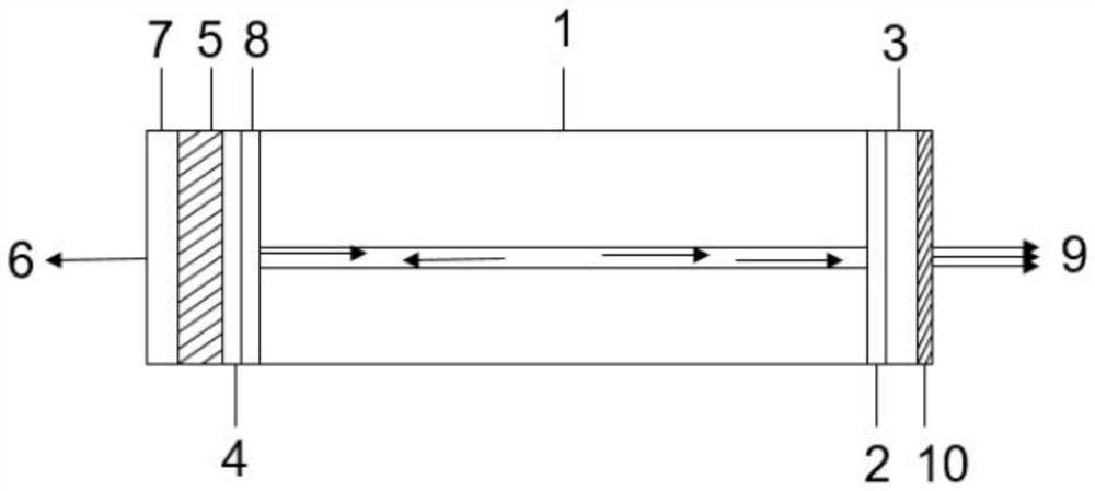
[0033] see figure 1 , the embodiment of the present invention provides a method for manufacturing a communication laser semiconductor chip, which includes the following steps: S1, stripping and clamping the wafer to be coated on the end face to obtain Bar bars, and processing them; The light-emitting cavity surface 9 of the bar is coated with three layers of high-transmission film systems in sequence, and the high-transmission film systems of the three layers ...


PUM

PropertyMeasurementUnit
thicknessaaaaaaaaaa
thicknessaaaaaaaaaa
thicknessaaaaaaaaaa

Abstract

The invention relates to the technical field of communication chip semiconductors, and provides a manufacturing method of a communication laser semiconductor chip. The method comprises the following steps of: S1, performing stripping and clamping on a wafer of which the end surface is to be coated to obtain a Bar strip, and processing the Bar strip; S2, sequentially coating the light emitting cavity surface of the to-be-plated Bar strip after treatment with three layers of high-transmittance film systems, wherein the three layers of high-transmittance film systems are respectively a first Si film, a first SiO film and a first SiO2: H film; and S3, after film coating of the light emitting cavity surface is completed, sequentially coating the backlight cavity surface of the Bar strip to be coated with four layers of high-reflection film systems, wherein the four layers of high-reflection film systems are a second SIO film, a second Si film, a second SiO2: H film and a third Si film respectively. The invention also provides the communication laser semiconductor chip. The chip is manufactured by the manufacturing method of the communication laser semiconductor chip. The end face film system adopts a pure Si multi-layer film, so that the lattice matching degree between film layers can be effectively improved, and the influence of excitons, defects and lattice vibration caused by high lattice mismatch ratio on the light absorption coefficient is reduced.

Description

technical field [0001] The invention relates to the technical field of communication chip semiconductors, in particular to a communication laser semiconductor chip and a manufacturing method thereof. Background technique [0002] At present, the manufacturing process of communication laser semiconductor chips is relatively mature. With the innovation and upgrading of the chip industry, the industry has put forward higher requirements for the speed and service life of communication chips. In order to improve the reliability of the chip, the requirements for the chip manufacturing process need to be higher Harsh, the end surface coating belongs to the end of the chip manufacturing process, and has a prominent impact on product reliability. Defects on the cavity surface, film growth energy, film compactness, film interface lattice mismatch ratio, and light absorption of materials will all affect product reliability. In particular, for high-speed Al-containing semiconductor mate...

Claims


Application Information

Patent Timeline
Patent Type & Authority Applications(China)
IPC IPC(8): H01S5/028
CPCH01S5/028H01S5/0282
Inventor 游顺青许海明
Owner 湖北光安伦芯片有限公司
Why Eureka
Try Eureka