Manufacturing method of light-emitting diode epitaxial wafer

A technology of light-emitting diodes and manufacturing methods, applied in the direction of electrical components, circuits, semiconductor devices, etc., can solve problems affecting the crystal quality of light-emitting diode epitaxial wafers, GaN layer warping, poor lattice matching, etc., and achieve improved sorting quality efficiency, lattice matching, and crystal quality

Active Publication Date: 2019-04-26
HC SEMITEK ZHEJIANG CO LTD
View PDF4 Cites 3 Cited by
  • Summary
  • Abstract
  • Description
  • Claims
  • Application Information

AI Technical Summary

Problems solved by technology

[0005] The surface of the AlN buffer layer formed by PVD equipment may be an N-polar plane, and the lattice matching between the N-polar plane and the GaN layer is poor, resulting i

Method used


Image

  • Manufacturing method of light-emitting diode epitaxial wafer
  • Manufacturing method of light-emitting diode epitaxial wafer
  • Manufacturing method of light-emitting diode epitaxial wafer

Examples


Embodiment Construction

[0034] In order to make the object, technical solution and advantages of the present invention clearer, the implementation manner of the present invention will be further described in detail below in conjunction with the accompanying drawings.

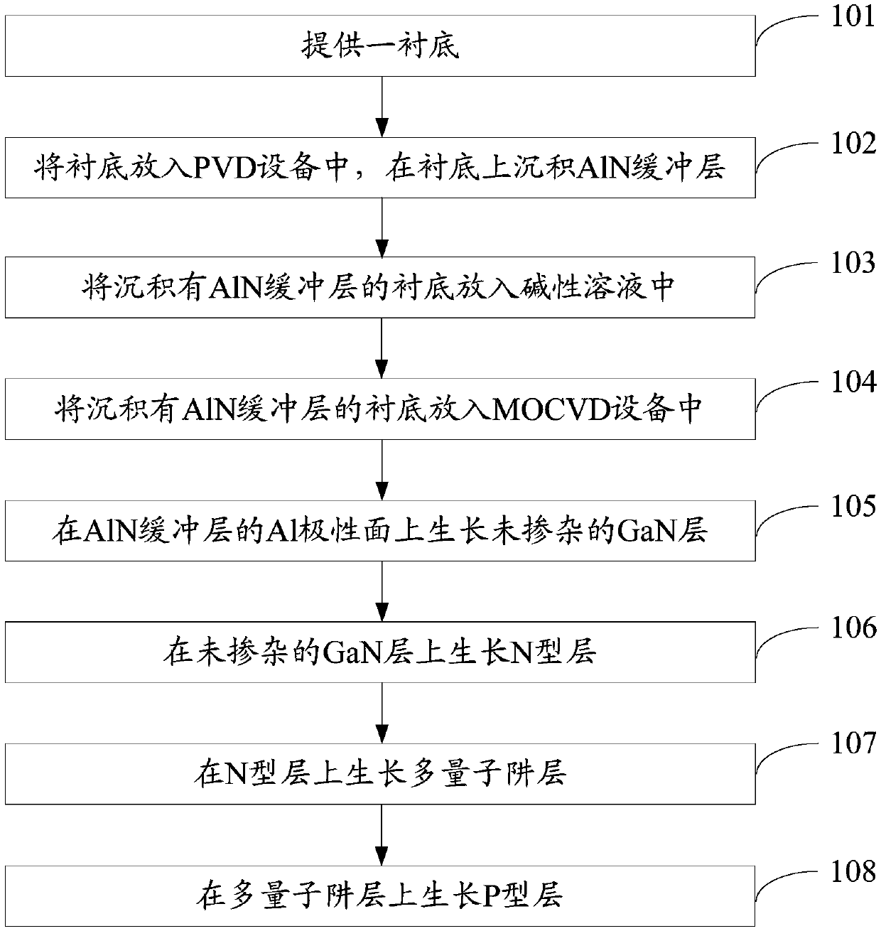
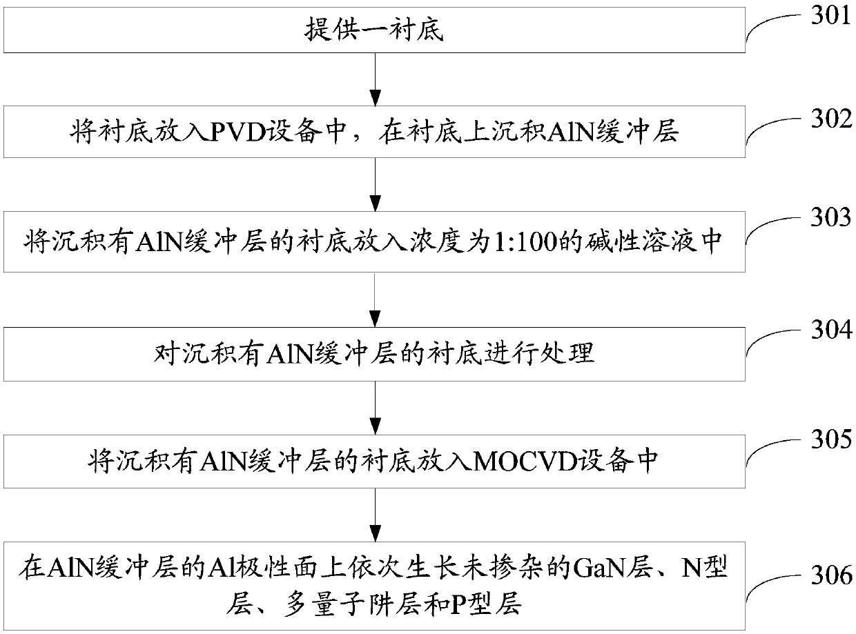
[0035] figure 1 It is a flow chart of a method for manufacturing a light-emitting diode epitaxial wafer provided by an embodiment of the present invention, as shown in figure 1 As shown, the manufacturing method includes:

[0036] Step 101, providing a substrate.

[0037] In this embodiment, the substrate may be a patterned sapphire substrate, Si substrate or SiC substrate.

[0038] Step 102, putting the substrate into a PVD device, and depositing an AlN buffer layer on the substrate.

[0039] In this embodiment, a magnetron sputtering method may be used to deposit an AlN buffer layer on the surface of the substrate.

[0040] Specifically, step 302 may include:

[0041] The pressure in the PVD chamber is controlled to be 4-10mtorr...


PUM


Abstract

The invention discloses a manufacturing method of a light-emitting diode epitaxial wafer, and belongs to the technical field of semiconductors. The manufacturing method comprises the following steps:providing a substrate; putting the substrate into PVD equipment, and depositing an AlN buffer layer on the substrate; putting the substrate deposited with the AlN buffer layer into an alkaline solution, and reacting the alkaline solution with the AlN buffer layer to ensure that the surface of the AlN buffer layer is an Al polar surface; putting the substrate deposited with the AlN buffer layer into MOCVD equipment, and sequentially growing an undoped GaN layer, an N-type layer, a multi-quantum well layer and a P-type layer on the Al polar surface of the AlN buffer layer. When the surface of the AlN buffer layer is an Al polar surface, the lattice matching degree between the AlN buffer layer and the undoped GaN layer is higher. Therefore, the manufacturing method can improve the lattice matching degree between the AlN buffer layer and the GaN layer, thereby improving the crystal quality of the grown light-emitting diode epitaxial wafer and further improving the luminous efficiency of the LED.

Description

technical field [0001] The invention relates to the technical field of semiconductors, in particular to a method for manufacturing a light-emitting diode epitaxial wafer. Background technique [0002] GaN (gallium nitride) has good thermal conductivity, high temperature resistance, acid and alkali resistance, high hardness and other characteristics, and is widely used in light-emitting diodes of various wavelengths. A core component of a GaN-based LED (Light Emitting Diode, light emitting diode) is an LED chip, and the LED chip includes an epitaxial wafer and electrodes disposed on the epitaxial wafer. [0003] The main structure of the GaN-based light-emitting diode epitaxial wafer includes: a substrate, and an AlN buffer layer, an undoped GaN layer, an N-type layer, a multi-quantum well layer and a P-type layer stacked on the substrate. In order to improve the production capacity of light-emitting diodes and the optoelectronic performance of LED chips, when the above-ment...

Claims


Application Information

Patent Timeline
IPC IPC(8): H01L33/00H01L33/12
CPCH01L33/007H01L33/12
Inventor 洪威威王倩董彬忠周飚胡加辉
Owner HC SEMITEK ZHEJIANG CO LTD
Why Eureka
Try Eureka