

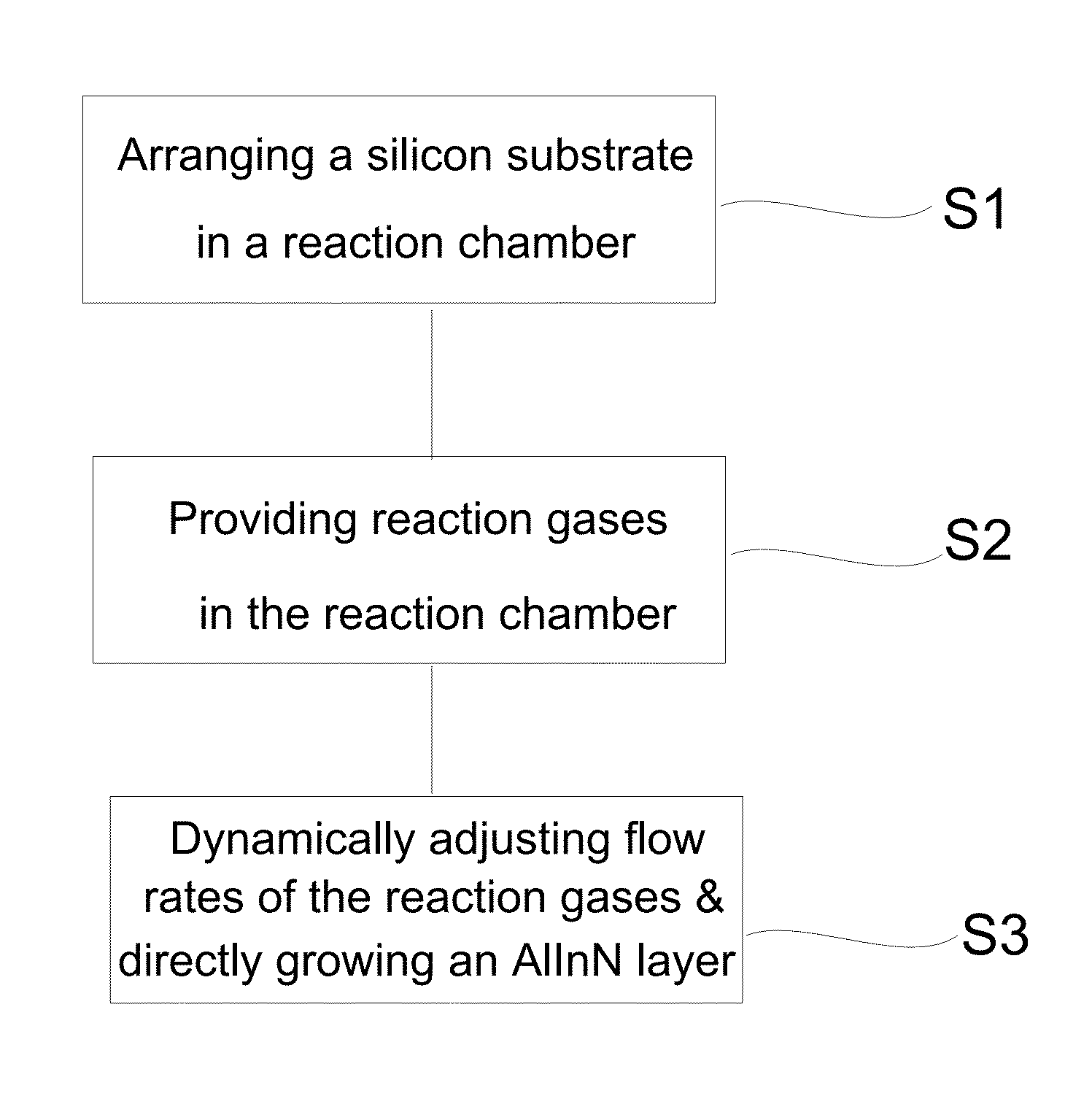
Method for growing aluminum indium nitride films on silicon substrate
- Summary
- Abstract
- Description
- Claims
- Application Information
AI Technical Summary
Benefits of technology
Problems solved by technology
Method used
Image

Examples
first example
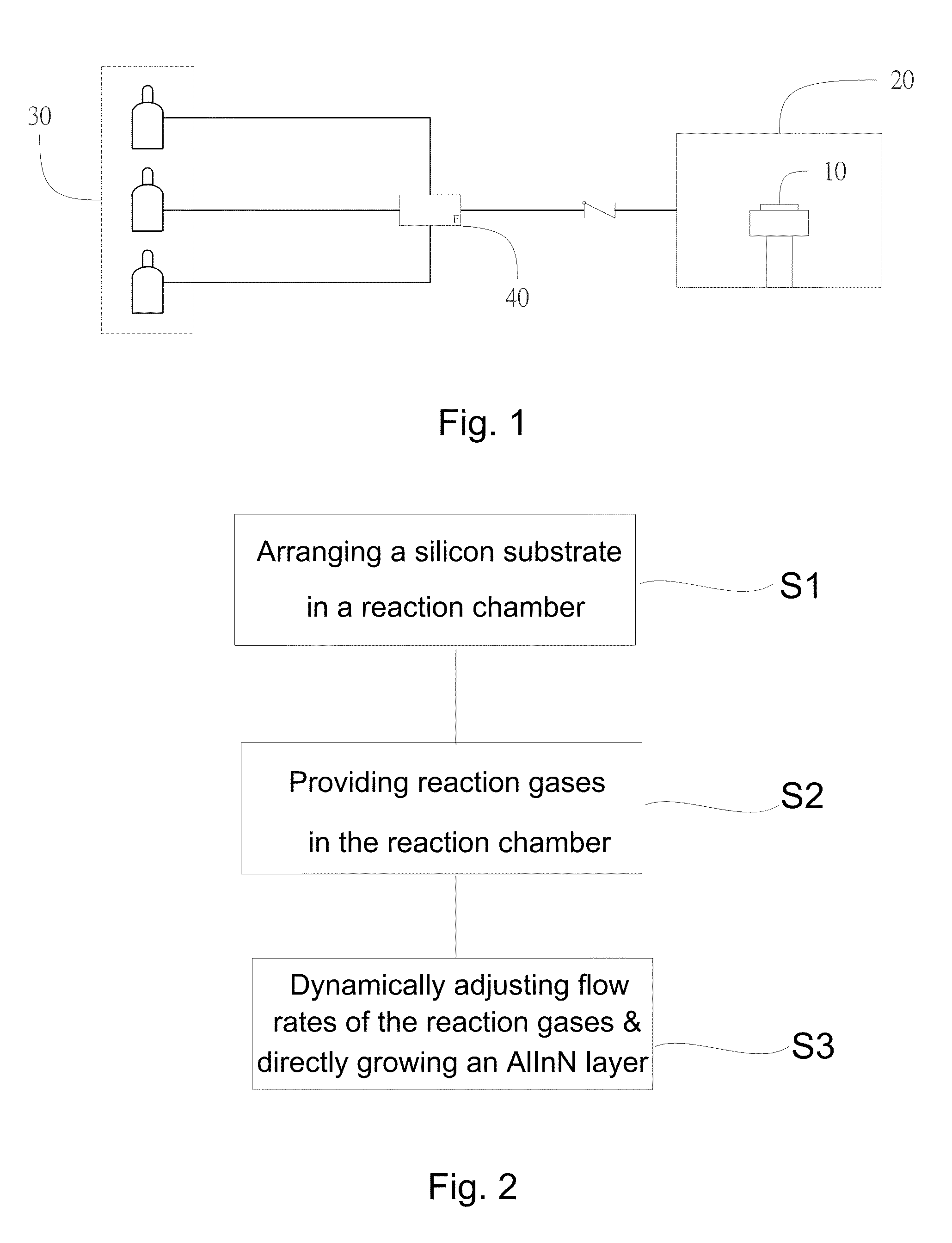
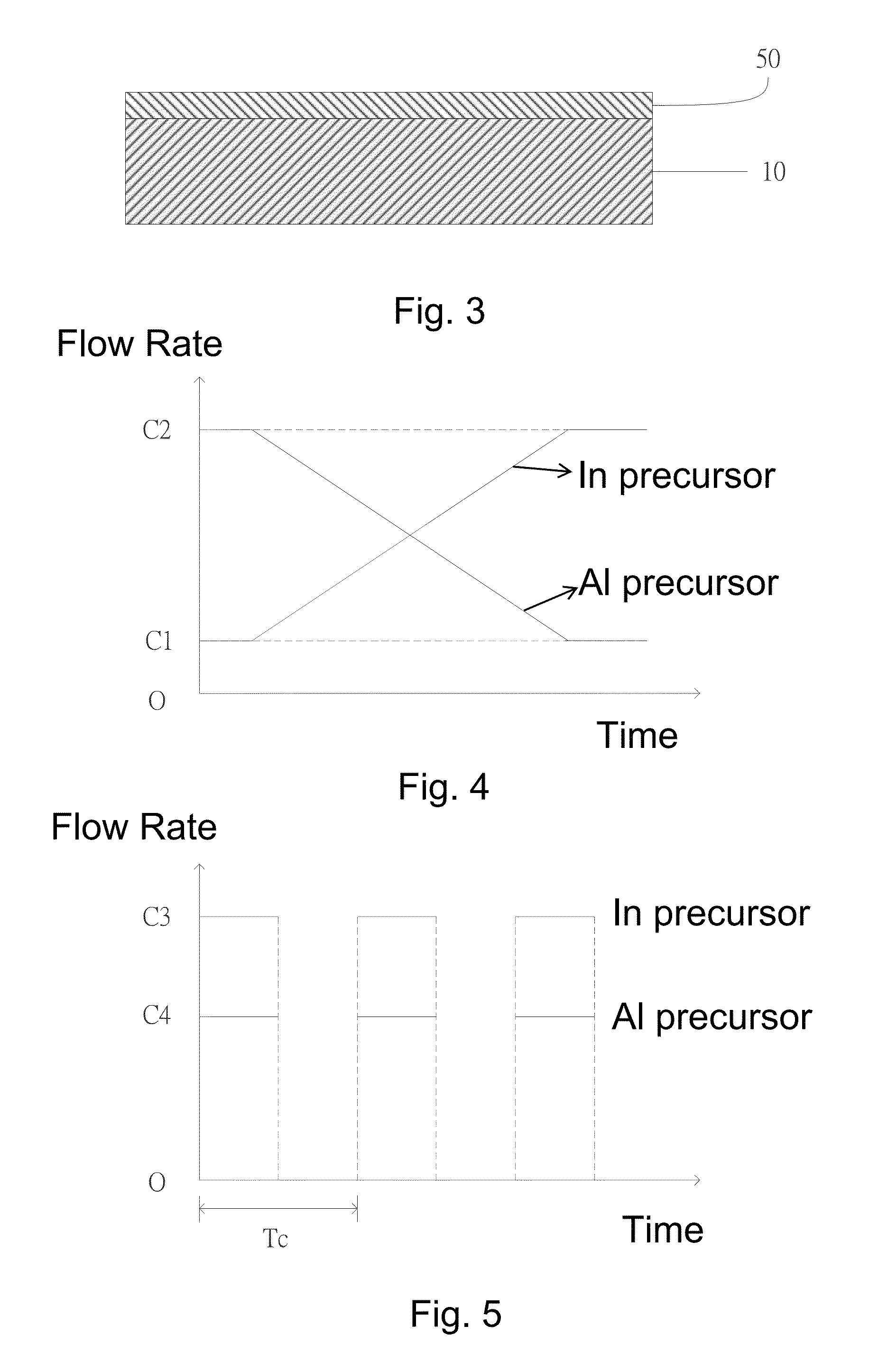
[0029]A Si(111) substrate is subjected to wet chemical cleaning by isopropanol, H2SO4 / H2O2 solution and DHF to remove contamination and oxidation layer on the substrate. Then the silicon substrate is arranged in the MOCVD reaction chamber. Hydrogen is provided and the silicon substrate is subjected to a thermal process at around 1000° C. After the temperature is decreased to 500° C. and the temperature and the pressure are balanced, organic metallic precursors containing trimethylaluminium (TMAl) and trimethylindium (TMIn) are provided into the chamber simultaneously according to a flow rate ratio of 10:1 by using hydrogen as a carrier gas. After seconds, when the surface of silicon substrate fully absorbs TMAl and TMIn, NH3 is provided under the same temperature and pressure to grow AlInN film. Afterwards, the flow rate of TMIn increases gradually such that the final flow rate ratio of TMAl and TMIn is 1:10. FIGS. 6A and 6B are surface and cross-sectional SEM micrographs after grow...
second example
[0030]Instead of Si(111) substrate used in the first embodiment, Si(110) substrate is used. The AlInN film is grown by the same method. 2θ-scan and Phi scan diagrams of AlInN(10-11) after growing AlInN film by X-ray diffraction (XRD) are shown in FIGS. 8A and 8B, respectively. The In content is about 76% in the film. Again, the AlInN film has a six-fold symmetrical structure. Therefore AlInN film can also be grown on the Si(110) substrate by epitaxy.
third example
[0031]Si(111) substrate is subjected to the same wet chemical cleaning as the first embodiment to be preprocessed. Then it is arranged in a radio frequency plasma-assisted metal-organic molecular beam epitaxy (RF-MOMBE) system to undergo a thermal process at 900° C. to remove oxidation layer on the surface of the substrate. The RF-MOMBE system excites provided nitrogen by RF (13.56 MHz) to produce plasma as a reaction source of nitrogen. The group III precursors of TMAl and TMIn are used for Al and In reaction sources, respectively. In this embodiment, the power is 300 W, flow rate of nitrogen is 1 sccm, working pressure −5 Torr, the flow rate ratio of TMIn / TMAl is a constant of 3.3. AlInN films are grown between 460° C.-550° C. by epitaxy. During the low temperature growing, TMIn and TMAl precursors are provided by a pulse cycle with providing precursors for 10 seconds and stop providing for 10 seconds in a cycle. 360 cycles are repeated. From 2θ-scan and Phi-scan diagrams of AlInN...
PUM
 Abstract
Description
Claims
Application Information