a ni-based 3 (hhtp) 2 Conductive thin film field effect transistor and its preparation method

A technology of field effect transistors and conductive thin films, applied in field effect transistors based on Ni32 conductive thin films and its preparation field, can solve the problem of poor contact between conductive thin films and device substrates and source and drain electrodes, poor uniformity of conductive thin films, heavy preparation Poor performance and other problems, to achieve the effect of improved carrier transport performance, good repeatability, and good uniformity

Active Publication Date: 2022-04-26
HEFEI INSTITUTES OF PHYSICAL SCIENCE - CHINESE ACAD OF SCI
View PDF8 Cites 0 Cited by
  • Summary
  • Abstract
  • Description
  • Claims
  • Application Information

AI Technical Summary

Problems solved by technology

[0006] In order to solve technical problems such as complex preparation process of field effect transistors in the prior art, poor preparation reproducibility, poor uniformity of conductive film, poor contact between conductive film and device substrate and source and drain electrodes, the invention provides a Ni-based 3 (HHTP) 2 Conductive thin film field effect transistor and its preparation method

Method used


Image

  • a ni-based  <sub>3</sub> (hhtp)  <sub>2</sub> Conductive thin film field effect transistor and its preparation method
  • a ni-based  <sub>3</sub> (hhtp)  <sub>2</sub> Conductive thin film field effect transistor and its preparation method
  • a ni-based  <sub>3</sub> (hhtp)  <sub>2</sub> Conductive thin film field effect transistor and its preparation method

Examples


preparation example Construction

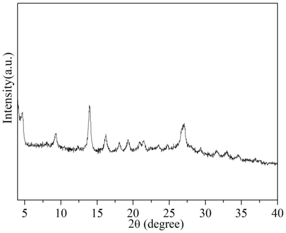
[0035] The invention provides a Ni 3 (HHTP) 2 The preparation method of conductive film can comprise the following steps:

[0036] Step 1. Adjust the pH value of the nickel acetate solution to 7.5-8.0, then add the hexahydroxytriphenylene ligand solution, and mix and stir (for example: it can be mixed and stirred for 3-8 minutes), so as to prepare Ni 3 (HHTP) 2 Reaction precursor.

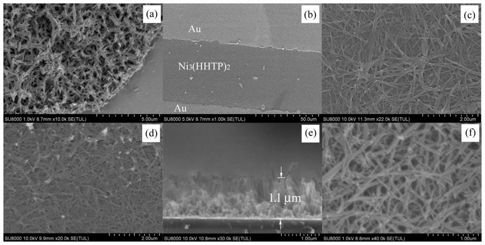
[0037] Step 2, the substrate (the substrate can be a silicon wafer substrate in the prior art, a silicon dioxide / silicon substrate (the silicon dioxide / silicon substrate refers to a substrate on which a layer of silicon dioxide is grown on the surface of a silicon wafer), Field effect transistor substrates including source, drain, gate three-terminal electrodes and channels, etc.) soak in nickel acetate solution with a concentration of 3.5 to 4.0 mg / mL for 3 to 5 minutes, and then take it out to dry (for example: it can be dried naturally or blown dry), and then suspend the dried substrate in t...

Embodiment 1

[0064] A Ni-based 3 (HHTP) 2 The field-effect transistor of conductive thin film, its preparation method comprises the following steps:

[0065] Step a1, select a silicon wafer with a silicon dioxide thickness of 280-300nm, soak it with ethanol and deionized water for ultrasound respectively, then spin-coat BP212-37S photoresist on the surface of the silicon wafer, pre-baked, and perform ultraviolet light according to the mask Engraving, development, post-baking after blowing dry with nitrogen, and then using magnetron sputtering to deposit an 80nm thick gold electrode layer on the silicon substrate, the channel length between the source and drain ends is 50 μm, and the width is 2000 μm; finally Soak ultrasonic waves in acetone for 40s, rinse and clean the surface of the device with ethanol and water, so as to prepare a field effect transistor substrate including source, drain, gate three-terminal electrodes and a channel.

[0066] Step a2, 30mg of nickel acetate tetrahydrat...

Embodiment 2

[0069] A Ni-based 3 (HHTP) 2 The field-effect transistor of conductive thin film, its preparation method comprises the following steps:

[0070] Step b1, select a silicon wafer with a silicon dioxide thickness of 280-300nm, soak it with ethanol and deionized water for ultrasound respectively, then spin-coat BP212-37S photoresist on the surface of the silicon wafer, pre-baked, and perform ultraviolet light according to the mask Engraving, development, post-baking after blowing dry with nitrogen, and then using magnetron sputtering to deposit an 80nm thick gold electrode layer on the silicon substrate, the channel length between the source and drain ends is 50 μm, and the width is 2000 μm; finally Soak ultrasonic waves in acetone for 40s, rinse and clean the surface of the device with ethanol and water, so as to prepare a field effect transistor substrate including source, drain, gate three-terminal electrodes and a channel.

[0071] Step b2, 30mg of nickel acetate tetrahydrat...


PUM

PropertyMeasurementUnit
concentrationaaaaaaaaaa
thicknessaaaaaaaaaa
widthaaaaaaaaaa

Abstract

The invention discloses a Ni-based 3 (HHTP) 2 Field-effect transistor of conductive thin film and preparation method thereof, the pH value of nickel acetate solution is adjusted to 7.5-8.0, and then hexahydroxytriphenylene ligand solution is added to mix and stir to prepare Ni 3 (HHTP) 2 Reaction precursor solution; the field effect transistor substrate including the source-drain-gate three-terminal electrode and the channel has the side of the channel facing down, suspended on the Ni 3 (HHTP) 2 React the surface of the precursor solution, and let it stand at 70-90°C for 2-5 hours to make a Ni-based 3 (HHTP) 2 Conductive thin-film field-effect transistors. The invention can make the conduction thin film and the base and the source and drain electrodes of the field effect transistor have good combination, make the field effect transistor have higher carrier mobility, and has simple operation, good preparation repeatability and uniform conduction thin film.

Description

technical field [0001] The invention relates to the field of field effect transistors, in particular to a Ni-based 3 (HHTP) 2 Conductive film field effect transistor and its preparation method. Background technique [0002] Ni 3 (HHTP) 2 It is a new type of two-dimensional conductive material with a metal-organic framework (MOF). Its structure has the characteristics of large specific surface area, porosity, adjustable structure, and many active sites. This graphene-like structure has attracted research and development in recent years. great attention from personnel. [0003] Typically, in 2D MOF conducting materials, conjugated organic ligands with chelating functional groups (e.g., –OH, –NH2, –SH, etc.) Connected with unpaired electrons, an extended p-conjugated structure is formed in the ab plane, and then these 2D lattices are stacked along the c direction through p–p interactions to form an ordered framework. The extended p-conjugated structure facilitates in-plan...

Claims


Application Information

Patent Timeline
Patent Type & Authority Patents(China)
IPC IPC(8): H01L51/40H01L51/30H01L51/05
CPCH10K71/15H10K85/331H10K10/468
Inventor 杨启段国韬罗媛媛高磊
Owner HEFEI INSTITUTES OF PHYSICAL SCIENCE - CHINESE ACAD OF SCI
Why Eureka
Try Eureka