SGT-MOSFET and manufacturing method thereof

A manufacturing method and deposition technology, applied in semiconductor/solid-state device manufacturing, electrical components, circuits, etc., can solve the problems of height difference, increase the complexity of contact hole etching process, and affect the accuracy of contact hole exposure, etc., to achieve Eliminate the effect of height difference

Pending Publication Date: 2021-10-01
SHANGHAI GREENPOWER ELECTRONICS
View PDF0 Cites 1 Cited by
  • Summary
  • Abstract
  • Description
  • Claims
  • Application Information

AI Technical Summary

Problems solved by technology

The disadvantage of this approach is that the height difference between the shielded gate polysilicon and the gate polysilicon is caused by photolithography on the wafer surface, and the height difference is about 1um, which will affect the subsequent photolithography process of the contact hole.
On the one hand, the height difference of polysilicon will affect the accuracy of contact hole exposure; on the other hand, since the length of the contact hole on the gate polysilicon, shield gate polysilicon, and substrate silicon surface is not the same, it will increase the contact hole etching. process complexity
[0004] Through the above analysis, the existing problems and defects of the prior art are: in the prior art, due to the height difference of the polysilicon on the surface of the wafer due to etching, it is easy to affect the photolithography process of the subsequent contact hole

Method used


Image

  • SGT-MOSFET and manufacturing method thereof
  • SGT-MOSFET and manufacturing method thereof
  • SGT-MOSFET and manufacturing method thereof

Examples


Embodiment Construction

[0058] In order to make the object, technical solution and advantages of the present invention more clear, the present invention will be further described in detail below in conjunction with the examples. It should be understood that the specific embodiments described here are only used to explain the present invention, not to limit the present invention.

[0059] Aiming at the problems existing in the prior art, the present invention provides a SGT-MOSFET and a manufacturing method thereof. The present invention will be described in detail below with reference to the accompanying drawings.

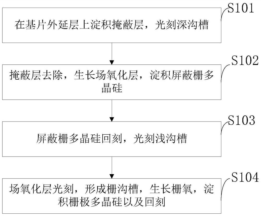
[0060] Those of ordinary skill in the industry of the manufacturing method of SGT-MOSFET provided by the present invention can also adopt other steps to implement, figure 1 The manufacturing method of the SGT-MOSFET provided by the present invention is only a specific embodiment.

[0061] Such as figure 1 As shown, the manufacturing method of the SGT-MOSFET provided by the embodiment of t...


PUM


Abstract

The invention belongs to the technical field of semiconductors, and discloses an SGT-MOSFET and a manufacturing method thereof. The method comprises the steps: depositing a masking layer on a substrate epitaxial layer, and photoetching a deep groove; removing the masking layer, growing a field oxide layer, and depositing shielding gate polycrystalline silicon; etching back shielding gate polycrystalline silicon, and photoetching a shallow groove; and photoetching a field oxide layer, forming a gate groove, growing a gate oxide layer, depositing gate polycrystalline silicon, performing back etching, and performing subsequent manufacturing. According to the invention, a new manufacturing method is adopted to connect the shield gate polycrystalline silicon and the gate polycrystalline silicon contact hole; and the manufacturing method adopted by the invention does not involve a photoetching process of shield gate polycrystalline silicon and grid polycrystalline silicon, and the shield gate polycrystalline silicon and the grid polycrystalline silicon are basically flush with the surface of the silicon substrate after being etched, so that the height difference of the polycrystalline silicon is eliminated, and the shield grid polycrystalline silicon and the grid polycrystalline silicon are punched well without generating the risk of bridging of the shield grid polycrystalline silicon and the grid polycrystalline silicon.

Description

technical field [0001] The invention belongs to the technical field of semiconductors, and in particular relates to an SGT-MOSFET and a manufacturing method thereof. Background technique [0002] At present, the traditional process steps of SGT are as simple as: first etch the epitaxial layer to form a deep trench, then grow a field oxide layer in the deep trench, and then fill the shielding gate polysilicon; then etch the field oxide layer to form a gate trench, Then a gate oxide layer is grown and filled with polysilicon to form a gate; finally, ion implantation in the well region and ion implantation in the source region form the source. For the specific SGT structure, see the top view and cross-sectional view of the SGT structure in the accompanying drawings. [0003] As the size of the device continues to shrink, due to the limitation of the size of the contact hole, it becomes more and more difficult to make a hole connection on the shielded gate polysilicon and the g...

Claims


Application Information

Patent Timeline
Patent Type & Authority Applications(China)
IPC IPC(8): H01L21/336H01L21/28H01L29/78H01L29/423
CPCH01L29/66484H01L21/28035H01L29/7831H01L29/4236H01L29/42376
Inventor 高学代萌
Owner SHANGHAI GREENPOWER ELECTRONICS
Why Eureka
Try Eureka