A kind of preparation method of circuit board for CCM module

A technology of circuit boards and modules, which is applied in the manufacture of printed circuits, assembly of printed circuits with electric components, printed circuits, etc., can solve the problems of affecting the flatness of chip attachment, increasing the thickness of circuit boards, and poor heat dissipation at the bottom, etc., to achieve Improve the excellent rate of the module, improve the heat dissipation, and the effect of small deformation

Active Publication Date: 2022-01-18
NINGBO HUAYUAN ELECTRONICS TECH
View PDF6 Cites 0 Cited by
  • Summary
  • Abstract
  • Description
  • Claims
  • Application Information

AI Technical Summary

Problems solved by technology

[0006] 3. The chip is attached to the surface of the solder resist, and the surface of the solder resist has a difference in height, which will affect the flatness of the chip attachment;
[0007] 4. The chip area is large, and the heat dissipation at the bottom is not good
In this structure, a high-temperature-resistant deformation-reinforcing layer is provided on the main body of the circuit board, and the photosensitive IC and the base are mounted on the high-temperature-resistant deformation-reinforcing layer. ability, so as to realize the smooth surface of the circuit board, but adding a high temperature resistant deformation reinforcement layer will inevitably increase the thickness of the circuit board, affect heat dissipation, and increase the production cost

Method used


Image

  • A kind of preparation method of circuit board for CCM module
  • A kind of preparation method of circuit board for CCM module
  • A kind of preparation method of circuit board for CCM module

Examples


Embodiment Construction

[0037] The present invention will be further described in detail below in conjunction with the accompanying drawings and embodiments.

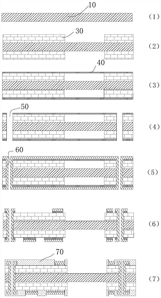
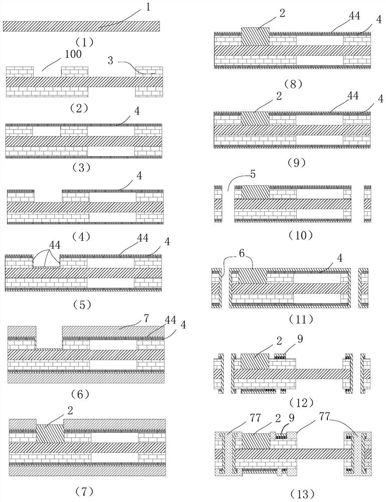
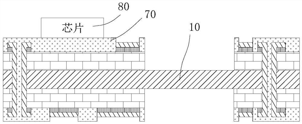
[0038] like figure 2 Shown, a kind of preparation method of circuit board for CCM module comprises the following steps:

[0039] 1) Fabrication of the inner core board 1: the inner core board 1 is made of a double-sided soft board pasted with a covering film;

[0040] 2) Lamination of the insulating layer 3: Laminate the prepreg of hard board epoxy resin and glass fiber cloth on the inner core board 1, and open the window 100 in advance corresponding to the chip area of ​​the inner core board 1, and the size ratio of the opening 100 The unilateral expansion of the copper pillar 2 is 0.14-0.16 mm; of course, other prepregs commonly used in this technical field can also be used for the prepreg;

[0041] 3) Bonding and pressing copper foil 4: Paste a layer of pure copper foil 4 on the surface of the insulating layer 3, and after lamination, th...


PUM

PropertyMeasurementUnit
thicknessaaaaaaaaaa

Abstract

A method for preparing a circuit board for a CCM module, the steps: making an inner core board; laminating the insulating layer: laminating and pressing copper foil; etching and opening: seed copper; exposure and development; electroplating copper pillars; after film removal Grinding; Drilling; Immersion Copper Plating; Outer Circuit Production; Solder Mask Production. The copper pillars are electroplated at the window, and the chip is directly attached to the copper pillars, which improves the heat dissipation. At the same time, the strength of the steel pillars determines the deformation of the chip. The chip undergoes a module assembly process, and the deformation in a high-temperature environment is negligible; the copper pillars After electroplating, a grinding process is added to make the surface smooth, and there is no height difference when the chip is attached; in addition, the chip is attached to the copper pillar, with small deformation, high resolution, and low paste failure. The process of the invention is simple and reasonable, and the prepared product not only has good heat dissipation performance and high flatness, but also has small deformation and high resolution rate, and effectively improves the excellent rate of the module.

Description

technical field [0001] The invention belongs to the technical field of circuit board production, and relates to a method for preparing a circuit board for a high-pixel CCM module. Background technique [0002] With the improvement of people's requirements for quality of life, photography or lighting has become an indispensable thing in people's life, and cameras and video cameras are also developing towards miniaturization, low power and low cost. [0003] CCM is the abbreviation of CMOS Camera Module. It is the core device used in various new generation portable camera equipment. Compared with the traditional camera system, it has the advantages of miniaturization, low power consumption, low cost and high image quality. However, with the improvement of pixels, the requirements for circuit boards are also getting higher and higher. The production of the existing high pixel CCM module circuit board is as follows: figure 1 As shown, the process is as follows: production of i...

Claims


Application Information

Patent Timeline
Patent Type & Authority Patents(China)
IPC IPC(8): H05K1/02H05K3/30H05K1/18
CPCH05K1/0209H05K3/303H05K1/181
Inventor 张成立徐光龙王强李东海茆昊奇黄礼树
Owner NINGBO HUAYUAN ELECTRONICS TECH
Why Eureka
Try Eureka