Heterojunction cell and preparation method thereof

A heterojunction cell, broadband technology, applied in circuits, photovoltaic power generation, electrical components, etc., to achieve good anti-reflection performance, improve contact performance, and improve short-circuit current effects

Active Publication Date: 2021-10-01
ANHUI HUASUN ENERGY CO LTD
View PDF4 Cites 1 Cited by
  • Summary
  • Abstract
  • Description
  • Claims
  • Application Information

AI Technical Summary

Problems solved by technology

[0004] Therefore, the technical problem to be solved by the present invention is to overcome the problem that the conversion efficiency of

Method used


Image

  • Heterojunction cell and preparation method thereof
  • Heterojunction cell and preparation method thereof
  • Heterojunction cell and preparation method thereof

Examples


Embodiment 1

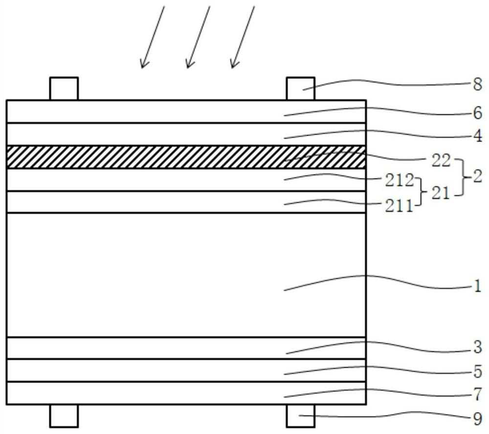
[0063] Please refer to figure 1 , figure 1 The middle arrow points to the irradiation direction of sunlight. In this embodiment, the intrinsic semiconductor composite layer 2 is only located on the front side of the semiconductor substrate layer 1 as an example for illustration.

[0064] In this case, preferably, the bandgap of the wide bandgap intrinsic layer 22 is 2.0eV˜9eV, for example, 2.0eV, 2.4eV, 2.8eV, 3.2eV and 9eV. Preferably, the ratio of the thickness of the wide bandgap intrinsic layer 22 to the thickness of the underlying intrinsic layer 21 is 1:1˜3:1, for example, 1:1, 2:1 or 3:1. Preferably, the thickness of the wide bandgap intrinsic layer 22 is 2nm-8nm, for example, 2nm, 5nm, 7nm or 8nm, and the thickness of the underlying intrinsic layer 21 is 1.3nm-3.3nm, for example, 1.3nm, 2nm , 3nm or 3.3nm.

[0065] The bottom intrinsic layer 21 includes: a first sub-bottom intrinsic layer 211; a second sub-bottom intrinsic layer 212 located on the surface of the fir...

Embodiment 2

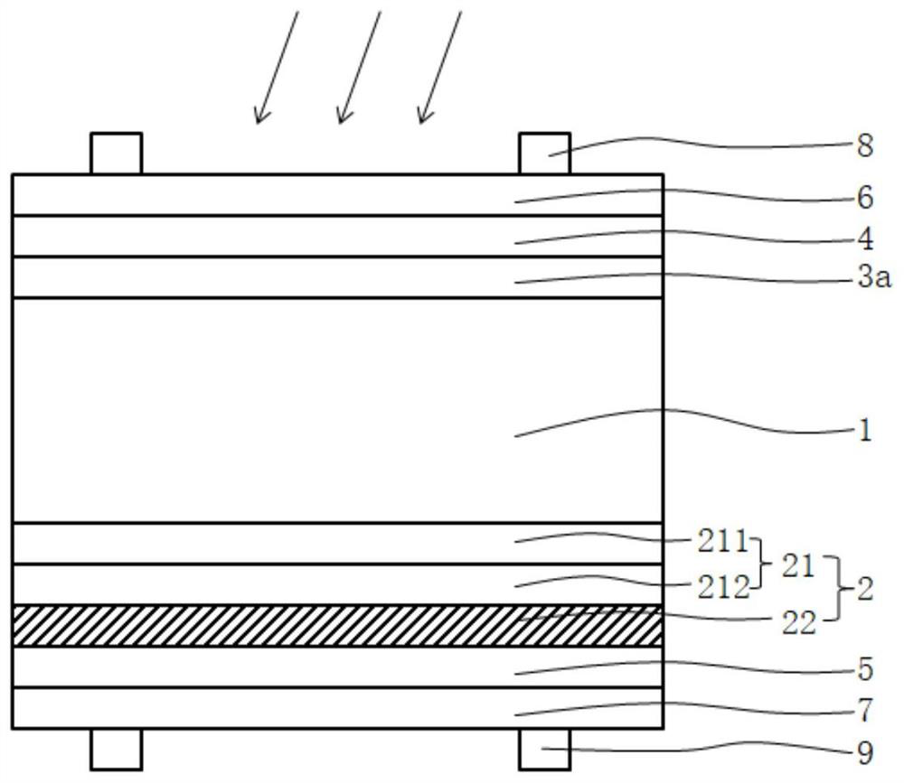
[0084] Please refer to figure 2 In this embodiment, the intrinsic semiconductor compound layer 2 is only located on the back side of the semiconductor substrate layer 1 as an example for illustration.

[0085] For the intrinsic semiconductor composite layer 2 located on the back side of the semiconductor substrate layer 1, the valence band difference between the intrinsic semiconductor composite layer 2 and the semiconductor substrate layer 1 is 0.6eV to 7.9eV, for example 0.6 eV, 1.0eV, 2.1eV, or 7.9eV.

[0086] Doping oxygen atoms or carbon atoms in the wide bandgap intrinsic layer 22 can improve the valence band difference between the intrinsic semiconductor composite layer 2 on the back side of the semiconductor substrate layer 1 and the semiconductor substrate layer 1, and the high valence band difference is beneficial to The accumulation effect of the hole carriers in the photogenerated carriers is enhanced, so that the open circuit voltage of the heterojunction cell i...

Embodiment 3

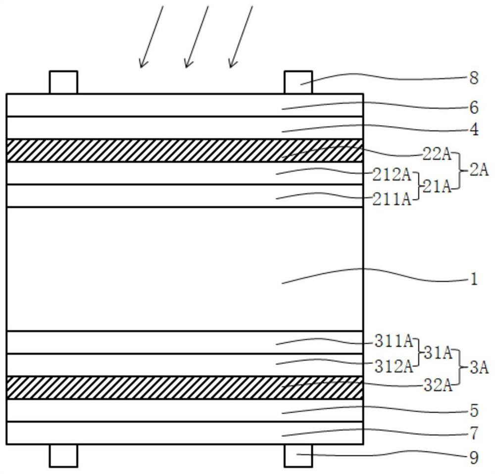
[0096] Please refer to image 3 In this embodiment, the intrinsic semiconductor composite layer is located on both sides of the semiconductor substrate layer 1, and the wide bandgap intrinsic layer is a single-layer structure (that is, N is equal to 1) as an example for illustration.

[0097] The intrinsic semiconductor composite layer includes a front intrinsic semiconductor composite layer 2A located on the front side of the semiconductor substrate layer 1 and a rear intrinsic semiconductor composite layer 3A located on the back side of the semiconductor substrate layer 1 .

[0098] The front intrinsic semiconductor composite layer 2A includes: the front bottom intrinsic layer 21A; the front wide bandgap intrinsic layer 22A located on the surface of the front bottom intrinsic layer 21A facing away from the semiconductor substrate layer 1, and the front wide bandgap intrinsic layer 22A. The bandgap of the intrinsic layer 22A is larger than the bandgap of the front bottom intr...


PUM

PropertyMeasurementUnit
Thicknessaaaaaaaaaa
Thicknessaaaaaaaaaa
Thicknessaaaaaaaaaa

Abstract

The invention provides a heterojunction cell and a preparation method thereof. The heterojunction cell comprises a semiconductor substrate layer and an intrinsic semiconductor composite layer. The intrinsic semiconductor composite layer is located on the surface of at least one side of the semiconductor substrate layer, and the intrinsic semiconductor composite layer comprises a bottom intrinsic layer and a wide-band-gap intrinsic layer located on the surface of the side, back on to the semiconductor substrate layer, of the bottom intrinsic layer, and the band gap of the wide-band-gap intrinsic layer is larger than that of the bottom intrinsic layer. The band gap of the wide-band-gap intrinsic layer is large, when sunlight irradiates the heterojunction cell, photons with energy smaller than that of the band gap of the wide-band-gap intrinsic layer cannot be absorbed in a parasitic mode, the parasitic absorption of the intrinsic semiconductor composite layer on the sunlight is reduced, and therefore the absorption of the semiconductor substrate layer on the sunlight is increased, photon-generated carriers generated by the semiconductor substrate layer are increased, so that the short circuit current of the heterojunction cell can be improved, and the conversion efficiency of the heterojunction cell can be improved.

Description

technical field [0001] The invention relates to the technical field of solar cell manufacturing, in particular to a heterojunction cell and a preparation method thereof. Background technique [0002] Solar cells are a kind of clean energy cells, and solar cells are widely used in life and production. Heterojunction solar cell is an important solar cell. The heterojunction (HeteroJunction with intrinsic Thin layer, HJT) structure is centered on the N-type monocrystalline silicon substrate, and the two sides of the N-type monocrystalline silicon substrate are respectively arranged P-type amorphous silicon layer and N-type amorphous silicon layer, add a layer of intrinsic amorphous silicon layer between the P-type amorphous silicon layer, N-type amorphous silicon layer and N-type single crystal silicon substrate, take the After the process measures, the passivation characteristics of the substrate silicon wafer are changed, thereby improving the conversion efficiency of the he...

Claims


Application Information

Patent Timeline
IPC IPC(8): H01L31/0288H01L31/0352H01L31/0747H01L31/20
CPCH01L31/0288H01L31/035281H01L31/202H01L31/0747Y02E10/50Y02P70/50Y02E10/548
Inventor 徐晓华辛科周肃龚道仁王文静李晨陈梦滢程尚之
Owner ANHUI HUASUN ENERGY CO LTD
Why Eureka
Try Eureka