

Probe card and wafer test system
A probe card and probe technology, applied in the field of probe cards, can solve the problems of inability to increase the test area and ensure the flatness of the tip of the probe, so as to improve the test efficiency and accuracy, and reduce the flatness requirements. The effect of area expansion
- Summary
- Abstract
- Description
- Claims
- Application Information
AI Technical Summary
Problems solved by technology
Method used
Image

Examples
Embodiment 1
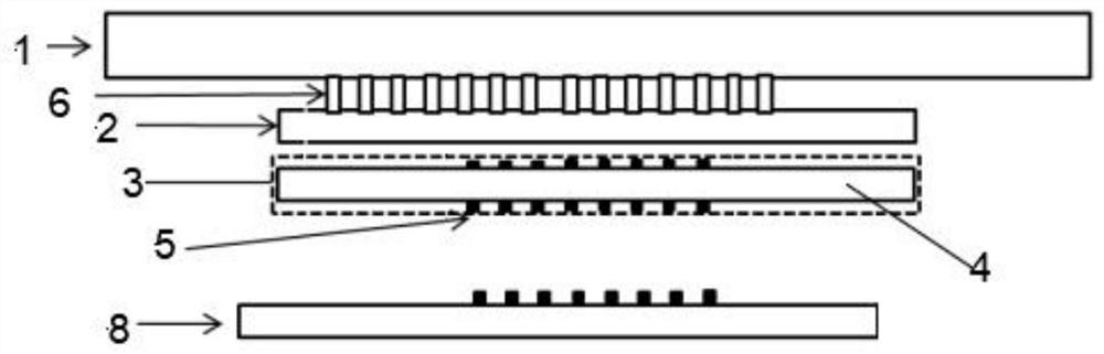
[0041] An embodiment of the present invention, such as figure 1 As shown, the present invention provides a probe card, including a PCB board 1 , a ceramic substrate 2 and a probe head 3 .
[0042] The ceramic substrate 2 is arranged on the PCB board 1 ; the probe head 3 is arranged on the ceramic substrate 2 , and the probe head 3 includes a guide plate 4 on which several uniformly distributed probes 5 are arranged.
[0043] Wherein, a plug board 6 is arranged between the PCB board 1 and the ceramic substrate 2, and a plurality of pogo pins passing through the plug board 6 are arranged on the plug board 6, and both ends of the pogo pins are fixedly connected with the PCB board 1 and the ceramic substrate 2 respectively.
[0044]Usually, the wafer test requires that the flatness of the tip of all probes (the flatness is the height difference of the tip) is less than 50um. Challenges; and with the test requirements of high test efficiency and high data throughput rate, the cust...
Embodiment 2
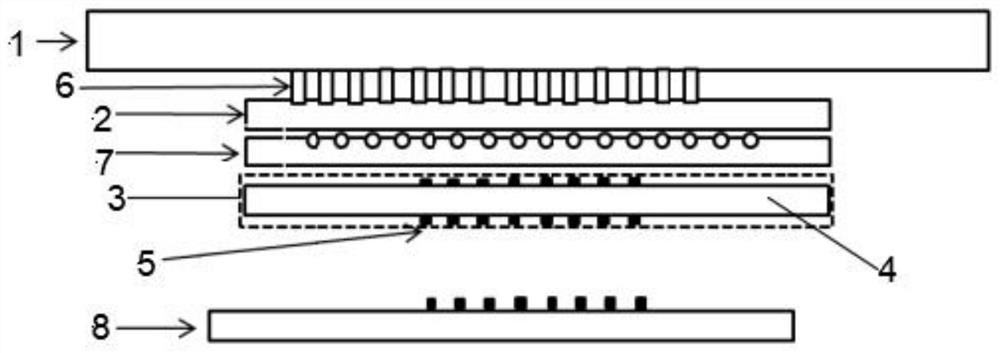
[0051] An embodiment of the present invention, such as figure 2 As shown, the present invention provides a probe card, including a PCB board 1 , a ceramic substrate 2 and a probe head 3 .
[0052] The ceramic substrate 2 is arranged on the PCB board 1 ; the probe head 3 is arranged on the ceramic substrate 2 , and the probe head 3 includes a guide plate 4 on which several uniformly distributed probes 5 are arranged.
[0053] Wherein, a plug board 6 is arranged between the PCB board 1 and the ceramic substrate 2, and a plurality of pogo pins passing through the plug board 6 are arranged on the plug board 6, and both ends of the pogo pins are fixedly connected with the PCB board 1 and the ceramic substrate 2 respectively.
[0054] An organic substrate 7 is disposed between the ceramic substrate 2 and the probe head 3 , and the organic substrate 7 is fixedly connected to the ceramic substrate 2 by way of circuit welding.
[0055] Usually, the wafer test requires that the flatne...
Embodiment 3
[0064] In an embodiment of the present invention, on the basis of Embodiment 1 or 2, the pogo pin includes a fixed section and a telescopic section, the fixed section is provided with an insertion hole, and the bottom end of the telescopic section is movably inserted into the insertion hole.
[0065] Specifically, when the fixed section and the telescopic section are connected, an external spring or an internal spring can be selected. When the spring is built in, a first spring can be arranged in the jack, and the two ends of the first spring are fixedly connected with the bottom end of the telescopic section and the bottom end of the jack respectively; An annular block is provided at the top of the telescopic section, and a second spring is sheathed outside the telescopic section, and the two ends of the second spring are respectively fixedly connected with the annular block and the top of the fixed section.
[0066] In addition, when connecting the PCB board and the ceramic ...
PUM
 Abstract
Description
Claims
Application Information