Formation method of semiconductor structure

A semiconductor and electromagnetic technology, applied in the direction of semiconductor devices, material selection, electric solid devices, etc., can solve problems such as poor performance of magnetic tunnel junctions

Pending Publication Date: 2021-10-12
SEMICON MFG INT (SHANGHAI) CORP +1
View PDF0 Cites 0 Cited by
  • Summary
  • Abstract
  • Description
  • Claims
  • Application Information

AI Technical Summary

Problems solved by technology

[0004] However, the performance of the magnetic tunnel junction prepared by the prior art is poor

Method used


Image

  • Formation method of semiconductor structure
  • Formation method of semiconductor structure
  • Formation method of semiconductor structure

Examples


Embodiment Construction

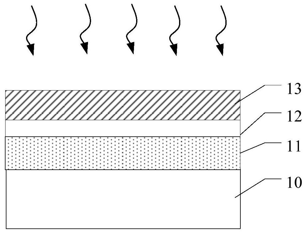
[0039] As mentioned in the background art, the performance of the magnetic tunnel junction prepared in the prior art is relatively poor. The reasons for the poor performance of the magnetic tunnel junction will be described in detail below with reference to the accompanying drawings.

[0040] Figure 1 to Figure 2 It is a structural schematic diagram of each step of a method for forming a semiconductor structure.

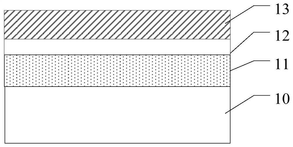
[0041] Please refer to figure 1 , a substrate 10 is provided, and the substrate 10 has a first electromagnetic film 11 , a tunnel film 12 on the surface of the first electromagnetic film 11 , and a second electromagnetic film 13 on the surface of the tunnel film 12 .

[0042] The first electromagnetic film 11 is used to form a first electromagnetic layer, the tunnel film 12 is used to form a tunnel layer, and the second electromagnetic film 13 is used to form a second electromagnetic layer. The first electromagnetic layer, tunnel layer , The second electromagneti...


PUM


Abstract

A forming method of a semiconductor structure comprises the following steps: providing a substrate; forming a first electromagnetic film on the substrate; forming a tunnel film on the surface of the first electromagnetic film; performing heat treatment on the first electromagnetic film and the tunnel film by adopting a first heating process; and after the first electromagnetic film and the tunnel film are subjected to heat treatment, forming a second electromagnetic film on the surface of the tunnel film. Therefore, the performance of the magnetic tunnel junction is improved.

Description

technical field [0001] The invention relates to the technical field of semiconductor manufacturing, in particular to a method for forming a semiconductor structure. Background technique [0002] MRAM (Magnetic Random Access Memory) is a non-volatile magnetic random access memory. It has the high-speed read and write capabilities of static random access memory (SRAM), high integration of dynamic random access memory (DRAM) and power consumption far lower than DRAM, compared with flash memory (Flash), with the use of time Increase performance without degradation. Due to the above-mentioned characteristics of MRAM, it is called universal memory and is considered to be able to replace SRAM, DRAM, EEPROM and Flash. [0003] Unlike traditional random access memory chip fabrication technology, data in MRAM is not stored in the form of charge or current, but in a magnetic state, and is sensed by measuring resistance without disturbing the magnetic state. MRAM uses a magnetic tunn...

Claims


Application Information

Patent Timeline
Patent Type & Authority Applications(China)
IPC IPC(8): H01L27/22H01L43/08H01L43/10H01L43/12
CPCH10B61/20H10N50/85H10N50/01H10N50/10
Inventor 郑二虎
Owner SEMICON MFG INT (SHANGHAI) CORP
Why Eureka
Try Eureka