Sacrificial silicon carbide seed crystal protective film

A silicon carbide seed and sacrificial technology, which is applied in the field of silicon carbide seed protective film, can solve the problems of crystal quality degradation, crystal scrapping, crystal unusability, etc., to achieve the purpose of suppressing volatilization, preventing excessive burn-through, and reducing volatilization Effect

Active Publication Date: 2021-10-15
SUZHOU UKING PHOTOELECTRIC TECH CO LTD
View PDF6 Cites 2 Cited by
  • Summary
  • Abstract
  • Description
  • Claims
  • Application Information

AI Technical Summary

Problems solved by technology

In most cases, the seed crystal will be burnt through before crystal growth, resulting in voids, which will extend until the end of crystal growth, resulting in defects such as micropipes and polycrystals in the crystal, and even the entire crystal is scrapped
[0005] At present, no measures have been found in the industry to protect the front of the seed crystal; the usual treatment for the back of the seed crystal is to bond graphite paper or carbon film to the back of the seed crystal, but it is difficult to eliminate the gap between the back of the seed crystal and the graphite paper. During the crystal growth process, the tiny air bubbles between them will still extend out of voids or micropipes, resulting in a decline in the quality of the crystal, and even the entire crystal cannot be used.

Method used


Image

  • Sacrificial silicon carbide seed crystal protective film
  • Sacrificial silicon carbide seed crystal protective film
  • Sacrificial silicon carbide seed crystal protective film

Examples


Embodiment 1

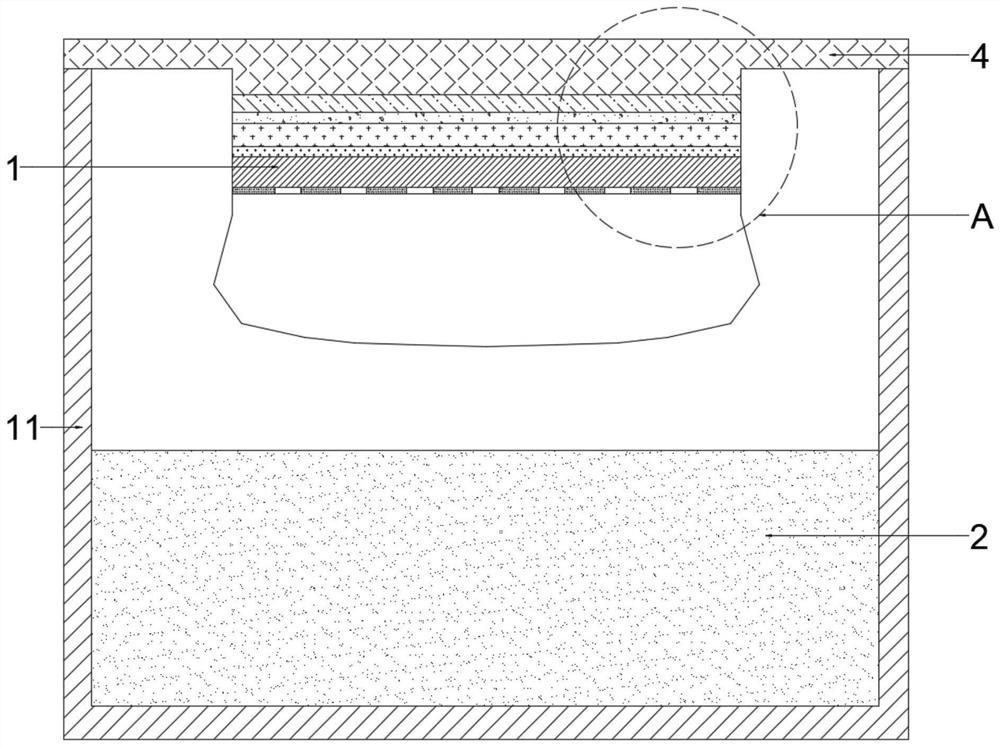
[0024] The growth of silicon carbide crystals is carried out in the silicon carbide growth chamber 11, the top of the silicon carbide growth chamber 11 is fixed with a seed crystal tray 4, the bottom of the silicon carbide growth chamber 11 is filled with silicon carbide raw materials 2, and the seed crystal 1 is fixed on the seed crystal tray 4. The bottom surface. In this embodiment, the side of the seed crystal 1 close to the seed crystal tray 4 is defined as the back side of the seed crystal 1, and the side of the seed crystal 1 close to the silicon carbide raw material 2 is defined as the front side of the seed crystal 1.

[0025] Such as figure 1 and figure 2 As shown, a sacrificial silicon carbide seed crystal protective film includes a first silicon carbide polycrystalline film 3 covering the front surface of the seed crystal 1 and a second silicon carbide polycrystalline film 5 covering the back surface of the seed crystal 1; that is The first silicon carbide polycr...

Embodiment 2

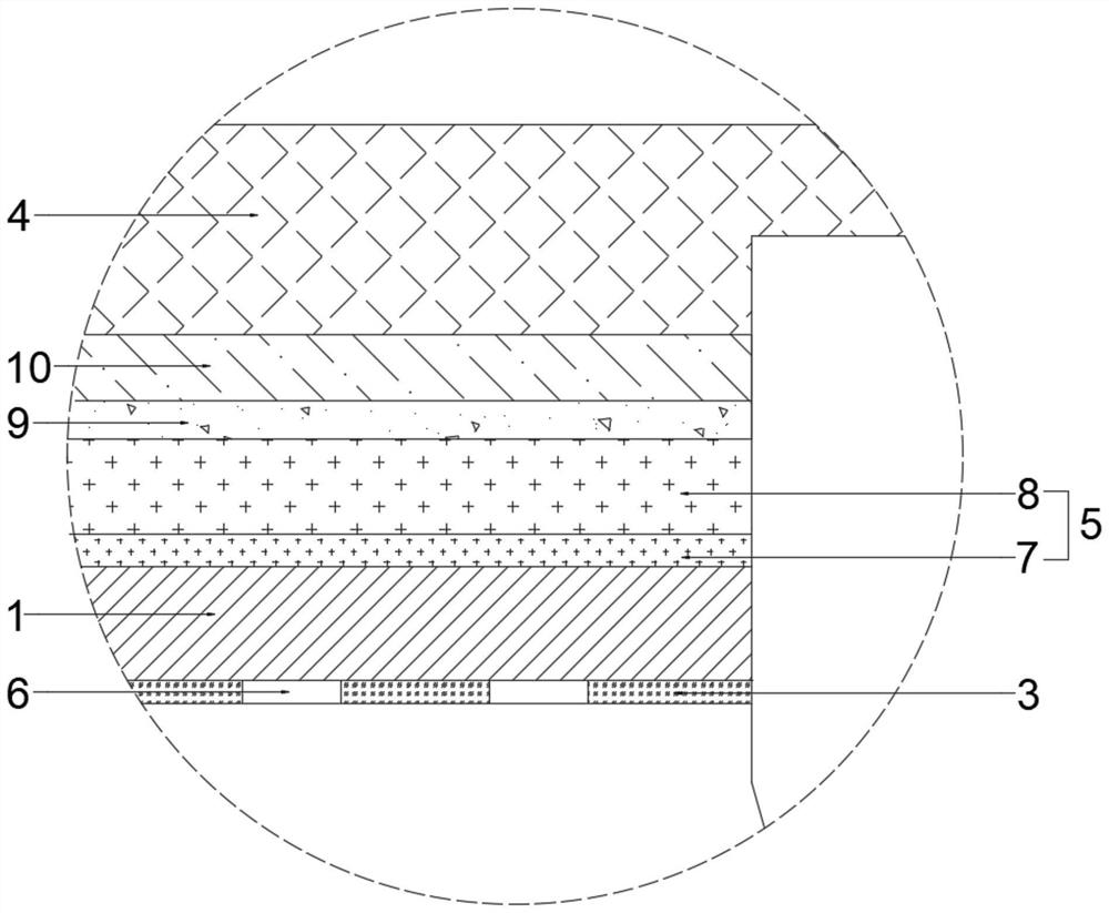
[0032] A sacrificial silicon carbide seed crystal protective film, comprising a first silicon carbide polycrystalline film 3 covering the front of the seed crystal 1 and a second silicon carbide polycrystalline film 5 covering the back of the seed crystal 1; the first Nanoscale through holes 6 are evenly distributed on the silicon carbide polycrystalline film 3; the second silicon carbide polycrystalline film 5 is a double-layer composite film, which sequentially includes a first film layer 7 and a second film layer 8; the seed crystal 1. A second silicon carbide polycrystalline film 5, a carbon film 9 and graphite paper 10 are sequentially pasted on the side close to the seed crystal tray 4, and the carbon film 9 is bonded to the graphite paper 10.

[0033] The first silicon carbide polycrystalline film 3 and the second silicon carbide polycrystalline film 5 cover the surface of the seed crystal 1 by directly reacting and sintering on the seed crystal 1 .

[0034]The binder i...

Embodiment 3

[0039] A sacrificial silicon carbide seed crystal protective film, comprising a first silicon carbide polycrystalline film 3 fixed on the front side of the seed crystal 1 and a second silicon carbide polycrystalline film 5 covering the back side of the seed crystal 1; the first Nanoscale through holes 6 are evenly distributed on the silicon carbide polycrystalline film 3; the second silicon carbide polycrystalline film 5 is a double-layer composite film, which sequentially includes a first film layer 7 and a second film layer 8; the seed crystal 1. A second silicon carbide polycrystalline film 5, a carbon film 9 and graphite paper 10 are sequentially pasted on the side close to the seed crystal tray 4, and the carbon film 9 and the graphite paper 10 are bonded together.

[0040] The first silicon carbide polycrystalline film 3 and the second silicon carbide polycrystalline film 5 cover the surface of the seed crystal 1 by directly reacting and sintering on the seed crystal 1 . ...


PUM

PropertyMeasurementUnit
thicknessaaaaaaaaaa
thicknessaaaaaaaaaa
particle diameteraaaaaaaaaa

Abstract

The invention provides a sacrificial silicon carbide seed crystal protective film which comprises a first silicon carbide polycrystalline film covering the front surface of the seed crystal and a second silicon carbide polycrystalline film covering the back surface of the seed crystal; nanoscale through holes are uniformly distributed in the first silicon carbide polycrystalline film; the second silicon carbide polycrystalline film is a double-layer composite film and sequentially comprises a first film layer and a second film layer; the back surface of the seed crystal is sequentially covered with the second silicon carbide polycrystalline film, a carbon film and graphite paper, and the second film layer is attached to the carbon film. As the defect density of the silicon carbide polycrystalline film is greater than that of the seed crystal, the silicon carbide polycrystalline film is volatilized preferentially in the heating process, and the generated gas is filled near the surface of the seed crystal, so that the volatilization speed of the surface of the seed crystal is delayed, and the seed crystal is protected. The carbon film is used for reducing the exposed area of the second film layer and delaying volatilization of the second film layer. The graphite paper has an isolation effect on the silicon carbide and the seed crystal tray, the stress of the seed crystal is reduced, and the seed crystal and the crystal are prevented from cracking.

Description

technical field [0001] The invention relates to a sacrificial silicon carbide seed crystal protective film, which belongs to the technical field of protective films. Background technique [0002] As the third-generation wide-bandgap semiconductor material, silicon carbide crystal has excellent properties such as high breakdown critical field strength, high electron saturation drift rate and high thermal conductivity, and can be widely used in the production of high-frequency, high-power, high-temperature-resistant power devices and in radio frequency devices. [0003] The industrial growth of silicon carbide crystals mainly adopts the physical vapor transport method (PVT method), that is, the silicon carbide raw material is heated and sublimated above 2100°C and decomposed to produce carbon source gas and silicon source gas, and the gas generated by the decomposition is transported to the seed crystal. Recrystallize to obtain a larger area of ​​silicon carbide (SiC) single ...

Claims


Application Information

Patent Timeline
Patent Type & Authority Applications(China)
IPC IPC(8): C30B29/36C30B23/00C30B28/02
CPCC30B29/36C30B23/00C30B28/02
Inventor 陈建明姜树炎周元辉刘春艳杨洪雨
Owner SUZHOU UKING PHOTOELECTRIC TECH CO LTD
Why Eureka
Try Eureka