A graphene plasmonic gas sensor and manufacturing method thereof
A technology of gas sensor and plasmon, applied in the field of plasmon gas sensor and its production, can solve the problems of low sensor sensitivity, low electrical response and Raman response, etc., to improve electrical response, improve Raman response, The effect of improving sensitivity
- Summary
- Abstract
- Description
- Claims
- Application Information
AI Technical Summary
Problems solved by technology
Method used
Image
Examples
Embodiment 1
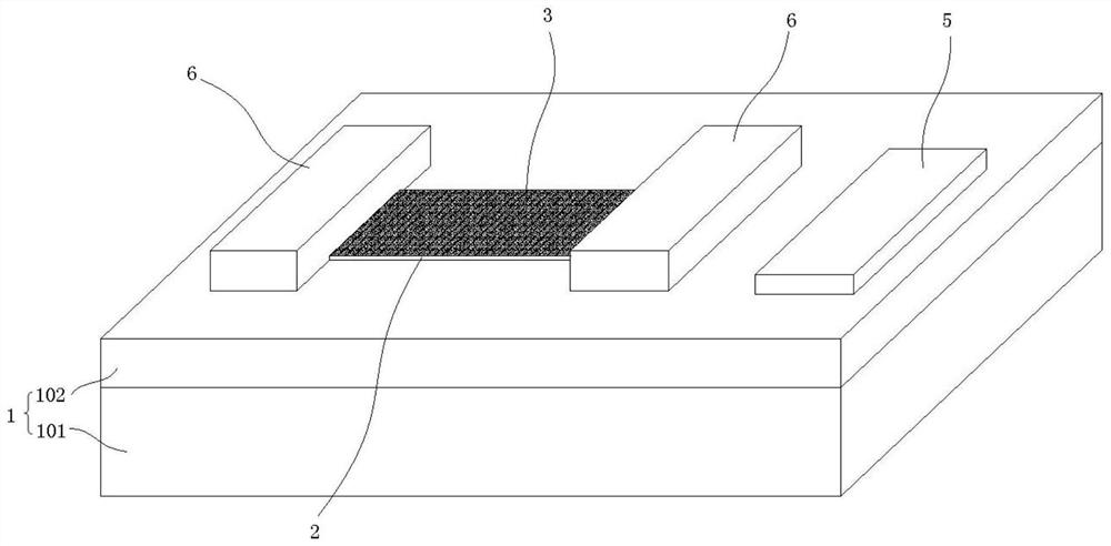
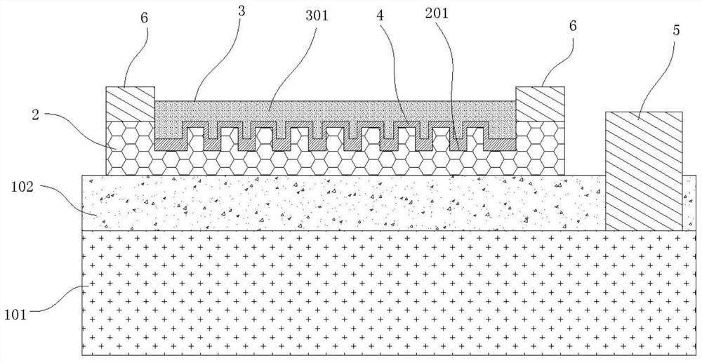
[0030] like figure 1 and figure 2 As shown, a graphene plasmonic gas sensor according to a preferred embodiment of the present invention includes a substrate 1, a graphene layer 2 and a noble metal particle layer 3, and the substrate 1, the graphene layer 2 and the noble metal particle layer 3 are in order from bottom to top It is provided that the noble metal particle layer 3 includes a plurality of noble metal particles 301 , and the noble metal particles 301 are located above the graphene layer 2 . In this embodiment, the graphene layer 2 and the noble metal particle layer 3 are sequentially arranged on the substrate 1 from bottom to top, so that the noble metal particles 301 can generate a surface-enhanced Raman (SERS) effect, thereby enhancing the interaction between graphene plasmons and gas molecules , to improve the Raman response of the graphene layer 2 to the gas, thereby obtaining a plasmon-enhanced Raman spectrum and improving the sensitivity of the sensor to gas...
Embodiment 2
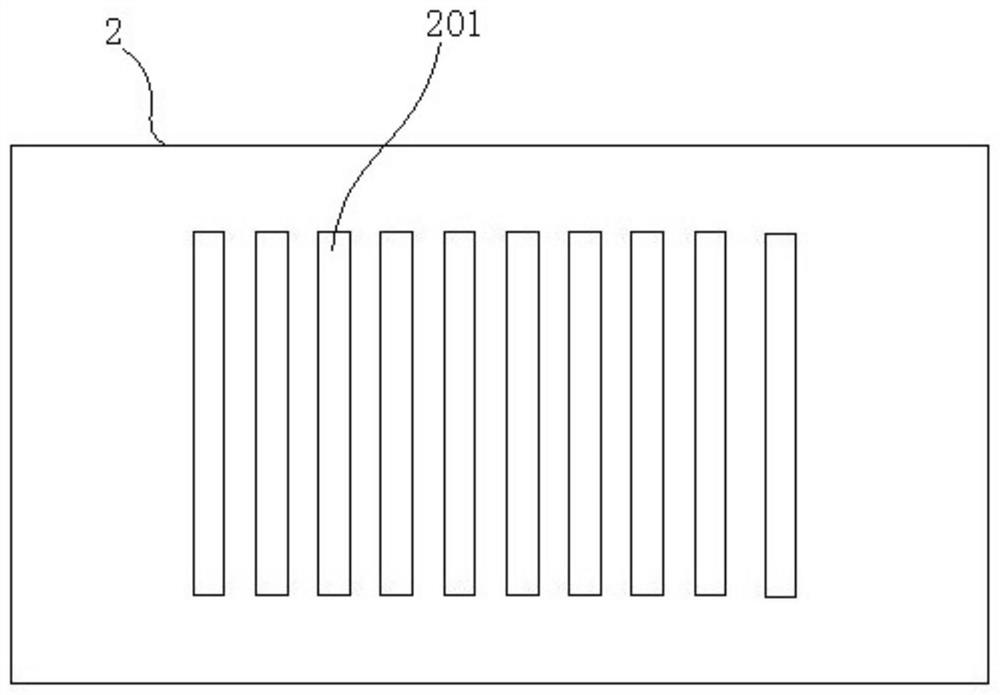
[0037] like Figure 4 As shown, the difference between this embodiment and the first embodiment is that the periodic nanostructure can also be a grid pattern, the grooves 201 are rectangular, and the plurality of grooves 201 are distributed in a rectangular array. After covering a graphene layer 2 on the substrate 1, it is etched away Figure 4 The rectangular part in the middle is formed with grooves 201, and a plurality of grooves 201 form periodic nanostructures. Other structures of this embodiment are the same as those of the first embodiment, and are not repeated here.
Embodiment 3
[0039] like Figure 5 As shown, this embodiment also provides a method for manufacturing a graphene plasmonic gas sensor, which includes the following steps:
[0040] Step S1, preparing a graphene layer on the upper surface of the substrate;
[0041] Step S2, depositing a precious metal layer on the graphene layer;
[0042] Step S3, preparing the noble metal particles of the noble metal layer into noble metal nanoparticles,
[0043] In step S1, a graphene film is first grown on a copper substrate by a CVD (chemical vapor deposition) method, and then the graphene film is transferred to SiO with a certain thickness 2 layer on the silicon substrate to form a graphene layer, which can be formed on SiO as needed 2 Layers arrange multiple graphene films from bottom to top. The area of graphene layer 2 is smaller than that of SiO 2 layer area so that the SiO 2 The layers have portions not covered by the graphene layer 2 . Then, by etching, the SiO 2 The part of the layer no...
PUM
| Property | Measurement | Unit |
|---|---|---|
| thickness | aaaaa | aaaaa |
| thickness | aaaaa | aaaaa |
| thickness | aaaaa | aaaaa |
Abstract
Description
Claims
Application Information


