High-quality waveguide structure and preparation method

A waveguide structure, high-quality technology, applied in the direction of optical waveguide light guide, light guide, instrument, etc., can solve the problems of unrealizable, excellent optical performance, etc., and achieve the effect of low transmission loss

Active Publication Date: 2021-10-22
EAST CHINA NORMAL UNIV
View PDF8 Cites 0 Cited by
  • Summary
  • Abstract
  • Description
  • Claims
  • Application Information

AI Technical Summary

Problems solved by technology

[0004] The purpose of the present invention is to overcome the problems that the pure chemical mechanical polishing process for preparing waveguides cannot achieve more excellent optical properties, and provide a waveguide structure and preparation method that can achieve excellent electro-optic performance, low loss, and good single-mode

Method used


Image

  • High-quality waveguide structure and preparation method

Examples


Embodiment 1

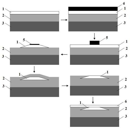
[0028] refer to figure 1 , the present invention utilizes femtosecond laser direct writing to combine chemical mechanical polishing technology and the method for preparing waveguide by bonding lithium niobate thin film to comprise the following steps:

[0029] (1) Prepare a lithium niobate wafer and plate a chromium film on its surface: take a 3-inch lithium niobate thin film wafer, which consists of a 300nm thick lithium niobate thin film 1 and a 4.7μm thick silicon dioxide layer 2 and a 0.5mm thick single crystal silicon substrate 3, and a chromium film 4 with a thickness of 400nm is plated on the surface of the lithium niobate film 1 by magnetron sputtering;

[0030] (2) Femtosecond laser direct writing chromium mask: Wipe the lithium niobate thin film wafer after the chromium coating layer 4 above with acetone to keep the cleanliness of the chromium film surface, and then fix it on a glass plate and absorb it with a suction cup Placed on a three-dimensional motion platfor...


PUM

PropertyMeasurementUnit
thicknessaaaaaaaaaa
thicknessaaaaaaaaaa
thicknessaaaaaaaaaa

Abstract

The invention discloses a high-quality waveguide structure and a preparation method thereof. The preparation method comprises the steps of plating a metal chromium film on the surface of a lithium niobate film, directly writing the chromium film by femtosecond laser as a mask layer, conducting chemical mechanical polishing, performing chemical vapor deposition, bonding the lithium niobate film and the like. The preparation process of the method optimizes the configuration of the waveguide prepared by the chemical mechanical polishing process, has the characteristic of ultralow transmission loss and excellent electro-optical characteristic, provides a key step for realizing industrialization of the lithium niobate photonic device, and can promote the development of micro-nano photonics, integrated optics and microwave photonics.

Description

technical field [0001] The invention relates to the field of on-chip integrated lithium niobate waveguide micro-nano preparation technology, in particular to a method for preparing a high-quality waveguide by using femtosecond laser direct writing combined with chemical mechanical polishing and lithium niobate thin film rebonding technology. The invention is suitable for preparing high-quality waveguide integrated structures on the surface of various thin film materials. Background technique [0002] With the rapid development of the information industry, traditional electronic chips are limited by Moore's Law and their electrons as information carriers, which may face huge challenges in the future; A breakthrough has been made in the field of transmission. At present, the silicon-based photonics technology with the silicon substrate on insulator as the core has achieved relatively mature development, but its development in nonlinear devices and electro-optic modulation dev...

Claims


Application Information

Patent Timeline
Patent Type & Authority Applications(China)
IPC IPC(8): G02B6/13G02B6/136G02B6/122
CPCG02B6/13G02B6/136G02B6/122
Inventor 程亚陈锦明
Owner EAST CHINA NORMAL UNIV
Why Eureka
Try Eureka