Supercharge Your Innovation With Domain-Expert AI Agents!

Microwave module integration design method, and microwave module produced by using method

A technology of microwave components and design methods, which is applied in the direction of waveguide devices, electrical components, circuits, etc., can solve the problems of high difficulty in assembly, high proportion of structural parts, and increased cost of circuit boards, so as to reduce the use of metal materials and reduce The difficulty of process assembly and the effect of reducing cost expenditure

Active Publication Date: 2021-11-02
ANHUI TIANBING ELECTRONICS TECH
View PDF6 Cites 0 Cited by
  • Summary
  • Abstract
  • Description
  • Claims
  • Application Information

AI Technical Summary

Problems solved by technology

[0008] The characteristics of the above design ideas are that the structural parts have better shielding effect and the product has higher firmness. In the bomb-loaded and airborne environment, it has the advantages of low deformation rate, strong impact resistance and stable performance; however, due to the structural parts of the product The specific gravity is high, and the space occupied in the volume is also relatively large. Correspondingly, the size of the circuit board is limited, and it cannot be realized with a single-layer circuit arrangement. The circuit board needs to be made into a multi-layer mixed voltage form. Integrated in a unit circuit board, the signal and DC interconnection between each unit circuit is carried out by using micro-connectors, which will inevitably lead to an increase in the cost of product structural parts and circuit board processing. At the same time, due to the extensive use of micro-shaped connectors, bring about a further increase in cost
For non-missile, airborne, even civilian vehicles, and other conditions that do not have strict requirements for the use environment, this design idea does not have a cost advantage, and the difficulty of assembly is high, and it is not manufacturable

Method used


Image

  • Microwave module integration design method, and microwave module produced by using method
  • Microwave module integration design method, and microwave module produced by using method
  • Microwave module integration design method, and microwave module produced by using method

Examples


Embodiment Construction

[0034] In order to make the technical means, creative features, goals and effects achieved by the present invention easy to understand, the present invention will be further described below in conjunction with specific embodiments.

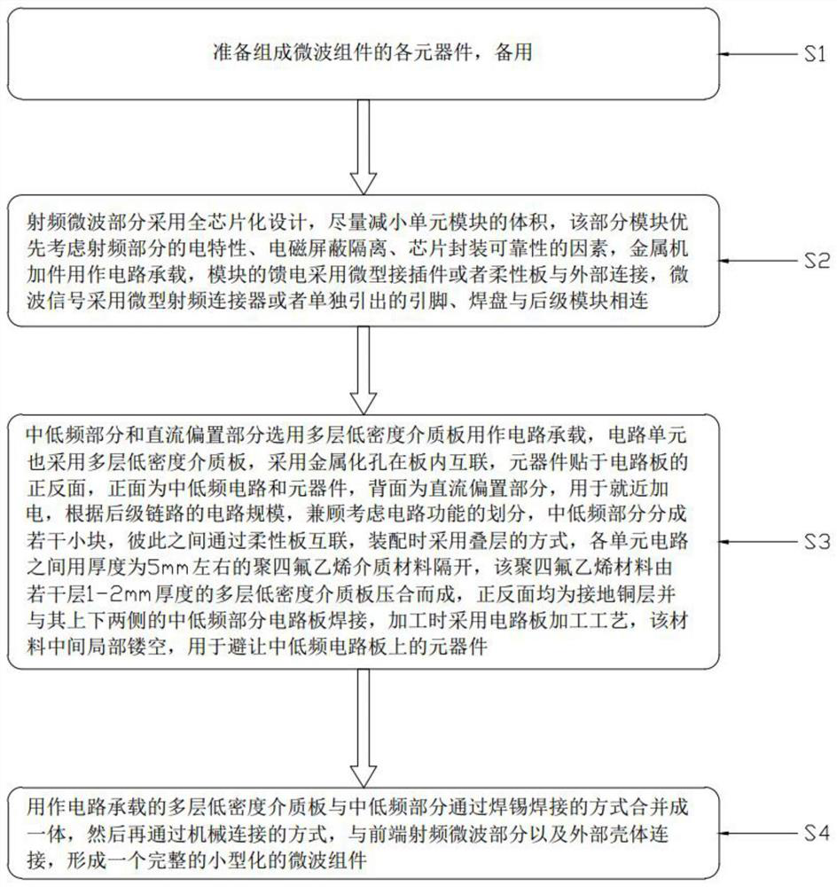
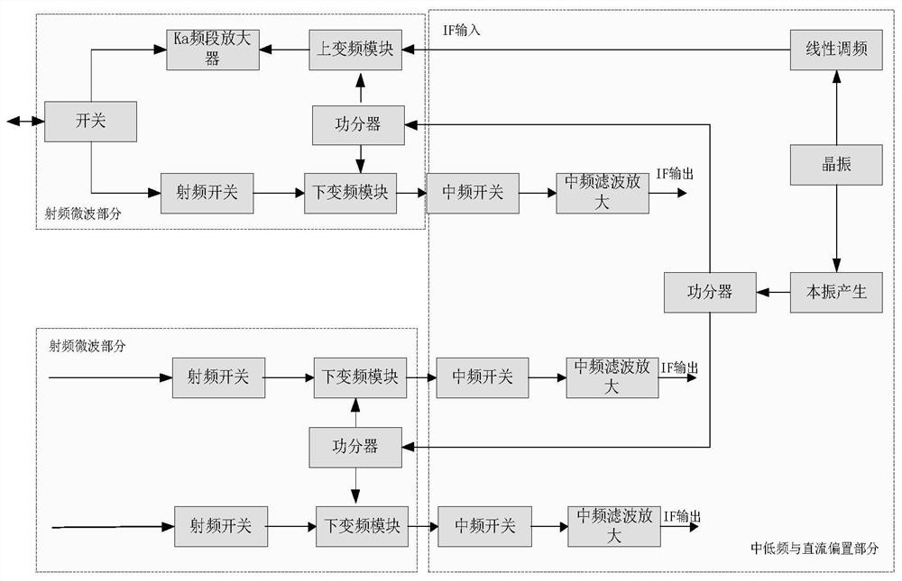
[0035] Such as figure 1 As shown, an integrated design method for microwave components, the unit circuit of the microwave component mainly includes a radio frequency microwave part, a medium and low frequency part, and a DC bias part from the perspective of the working frequency band;

[0036] The integrated design method of the above-mentioned microwave components includes the following steps:

[0037] S1. Prepare the various components that make up the microwave assembly and set them aside;

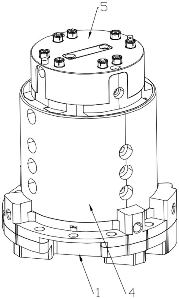
[0038] S2. The radio frequency and microwave part adopts a full-chip design to minimize the volume of the unit module. This part of the module gives priority to the electrical characteristics of the radio frequency part, electromagnetic shielding and isola...


PUM


Abstract

The invention discloses a microwave module integration design method, and a microwave module produced by using the method, and relates to the field of communication equipment. The method comprises the following steps: preparing components, manufacturing a radio frequency microwave part, manufacturing a low and medium frequency part and a direct current bias part, and assembling the module. Epoxy dielectric plates with different thicknesses are processed into special shapes by means of circuit board processing, mixed pressing, forming and copper coating processing technologies, and are combined into an expected design shape by means of a sintering assembly technology to be used as a bearing body of a unit electrical performance circuit board to replace a metal structural part, so that the use of metal materials can be reduced to a certain extent, and the processing cost of the metal part is reduced.

Description

technical field [0001] The invention belongs to the field of communication equipment, and in particular relates to an integrated design method of a microwave component and a microwave component produced by applying the method. Background technique [0002] With the further development of the current microwave technology, the miniaturization and high integration requirements of microwave products are getting higher and higher. Within the limited volume, more comprehensive functions must be integrated as much as possible to ensure that the product can be reduced in size as much as possible. While the weight and cost are limited, it can exert greater performance within limited conditions. [0003] For the current microwave products, most of them are composed of metal structural parts, single-layer dielectric boards or mixed-pressure dielectric boards, chips and packaging components. The product structure idea is generally as follows: [0004] 1. As the structural main body of...

Claims


Application Information

Patent Timeline
IPC IPC(8): H01P11/00
CPCH01P11/00
Inventor 张东响
Owner ANHUI TIANBING ELECTRONICS TECH
Features
  • R&D
  • Intellectual Property
  • Life Sciences
  • Materials
  • Tech Scout
  • Unparalleled Data Quality
  • Higher Quality Content
  • 60% Fewer Hallucinations
Learn More