High-extensibility electrolytic copper foil and preparation method thereof
An electrolytic copper foil, high extensibility technology, applied in the direction of electrolysis, electroforming, manufacturing tools, etc., can solve the problems of copper foil ductility, strength and cost can not be balanced, to achieve low production cost, high tensile strength, easy-to-achieve effects
- Summary
- Abstract
- Description
- Claims
- Application Information
AI Technical Summary
Problems solved by technology
Method used
Image
Examples
Embodiment 1
[0034] The method for preparing (111) textured high-extensibility electrolytic copper foil in this example is as follows: firstly, nano-twinned copper foil is prepared by DC electrodeposition technology, and then nano-twinned copper foil is annealed. The specific process is as follows:
[0035] 1. Preparation of nano-twinned copper foil by DC electrodeposition technology:
[0036] Electrolytic deposition equipment: DC stabilized voltage and stabilized current power supply;
[0037] Electrolyte composition for electrolytic deposition: CuSO 4 100g / L, analytical pure gelatin 40mg / L, HCl 40 mg / L, use deionized water to prepare electrolyte, use analytical pure H 2 SO 4 Adjust the pH of the electrolyte to 1.
[0038] The anode and cathode are iridium tantalum titanium plate and pure titanium plate respectively.
[0039] Electrolytic deposition process parameters: DC electrolytic electroplating copper foil, the current density is 30mA / cm 2 The distance between the cathode and th...
Embodiment 2
[0046] The difference from Example 1 is:
[0047] Annealing conditions: the annealing temperature is 450° C., and the annealing time is 10 minutes.
[0048] The prepared high-extensibility electrolytic copper foil has a thickness of 11.7 μm measured by the weighing method, and is characterized in that: the average number of crystal grains distributed along the thickness direction of the copper foil is 6.3, and the copper foil is paralleled by the intercept method. The surface statistical grain size, the average grain size is 1.1 microns, the ratio of thickness to grain size is 10.6. There is a twinned lamellar structure inside the grain, and the average thickness of the twinned lamellar layer is 0.3 microns obtained by statistics of the perpendicular direction of the twinned grain boundary by the intercept method, as shown in Figure 4 shown.
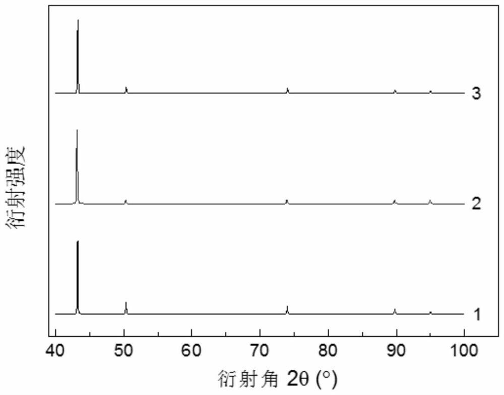
[0049] The prepared electrolytic copper foil has a strong (111) texture, such as figure 2 Shown in curve 2.
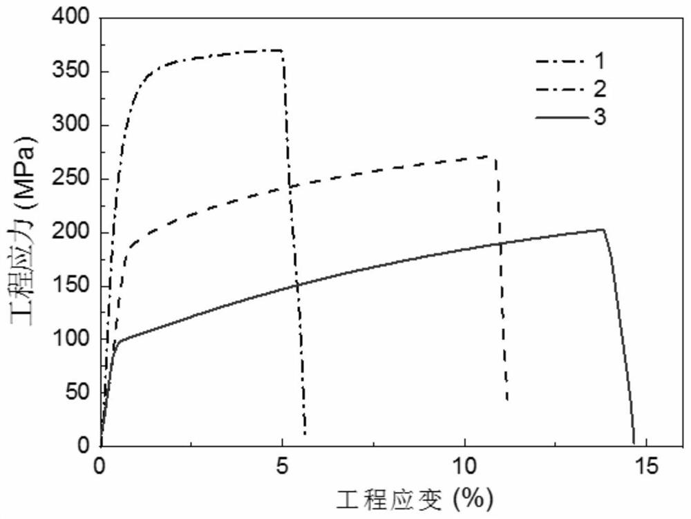
[0050] In this exampl...
Embodiment 3
[0052] The difference from Example 1 is:
[0053] Annealing conditions: the annealing temperature is 500° C., and the annealing time is 10 minutes.
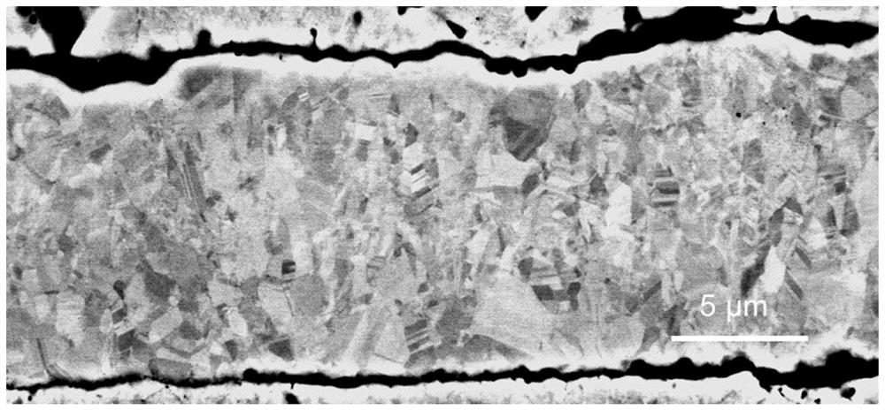
[0054] The prepared electrolytic copper foil has a thickness of 12.4 μm measured by the weighing method, and is characterized in that: the average number of crystal grains distributed along the thickness direction of the copper foil is 2.4, and the crystal grains are counted parallel to the surface of the copper foil by the intercept method. Grain size, the average grain size is 5.0 microns, and the ratio of thickness to grain size is 2.5. There is a twinned crystal layer structure inside the grain, and the average twinned crystal layer thickness is 0.74 microns obtained by statistics of the perpendicular direction of the twinned grain boundary by the intercept method, as shown in Figure 5 shown.
[0055] The prepared electrolytic copper foil has a strong (111) texture, such as figure 2 Shown in curve 3.
[0056] In this ex...
PUM
| Property | Measurement | Unit |
|---|---|---|
| Thickness | aaaaa | aaaaa |
| Average grain size | aaaaa | aaaaa |
| Thickness | aaaaa | aaaaa |
Abstract
Description
Claims
Application Information


