Novel multi-topology DC voltage converter for DC micro-grid
A technology of DC microgrid and DC voltage, which is applied in the direction of converting DC power input to DC power output, adjusting electrical variables, and AC network circuits. Rich bottom-level control experiment environment, safe DC voltage conversion, and space-saving effects
- Summary
- Abstract
- Description
- Claims
- Application Information
AI Technical Summary
Problems solved by technology
Method used
Image

Examples
Embodiment 1
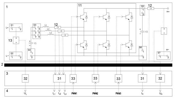
[0031] Regarding the one-way and two-way control of BOOST, by connecting the No. 2 pin of the first terminal S1 and the No. 4 pin of the third terminal S3, the No. 2 pin of the second terminal S2 and the No. 2 pins, No. 1 pins and No. 2 pins of the fifth connection terminal S5 constitute as figure 2 The BOOST structure connection diagram shown in the figure, the user connects the positive and negative ends of the low-voltage side unidirectional or bidirectional power supply to the No. 1 pin of the first terminal S1 and the No. 1 pin of the second terminal S2 on the power layer 1, respectively. , connect the load on the high-voltage side or the positive and negative ends of the power supply to H+ and H- respectively; at the control layer 4, the user collects I L1 and U H The signal can be adjusted through PWM1, and the user can perform closed-loop control of the output side voltage with sudden changes in the input voltage; through connecting the No. 1 pin and No. 4 pin of the...
Embodiment 2
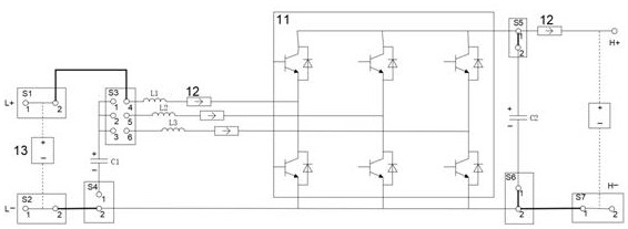
[0033] Regarding the one-way and two-way control of BUCK, by connecting pin No. 2 of the first terminal S1 and pin No. 4 of the third terminal S3, pin No. 1 and pin 4 of the third terminal S3, The No. 2 pin of the second connecting terminal S2 and the No. 1 pin of the fourth connecting terminal S4, the No. 1 pin and the No. 2 pin of the sixth connecting terminal S6 can be formed as follows image 3 The connection diagram of the BUCK structure shown in the figure, the user connects the positive and negative ends of the low-voltage side load or power supply to the No. 1 pin of the first terminal S1 and the No. 1 pin of the second terminal S2 on the power layer 1, respectively. Connect the positive and negative ends of the unidirectional or bidirectional power supply on the high-voltage side to H+ and H- respectively; at the control layer 4, the user collects the I H and U L The signal can be adjusted through PWM1, and the user can perform closed-loop control of the output side ...
Embodiment 3
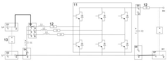
[0035] Regarding the one-way and two-way control of BUCK / BOOST, by connecting the No. 2 pin of the first terminal S1 and the No. 1 pin of the third terminal S3, and the No. 1 pin and the No. 4 pin of the third terminal S3 , No. 4 pin of the third connecting terminal S3 and No. 1 pin of the seventh connecting terminal S7 can be constituted as follows Figure 4 The connection diagram of the BUCK structure shown in the figure, the user connects the positive and negative ends of the low-voltage side load or power supply to the No. 1 pin of the first terminal S1 and the No. 1 pin of the second terminal S2 on the power layer 1, respectively. Connect the positive and negative ends of the unidirectional or bidirectional power supply on the high-voltage side to H+ and H- respectively; at the control layer 4, the user collects I H and U L The signal can be adjusted through PWM1, and the user can perform closed-loop control of the output side voltage for sudden changes in the input volt...
PUM
 Abstract
Description
Claims
Application Information
 - R&D
- Intellectual Property
- Life Sciences
- Materials
- Tech Scout
- Unparalleled Data Quality
- Higher Quality Content
- 60% Fewer Hallucinations
Browse by: Latest US Patents, China's latest patents, Technical Efficacy Thesaurus, Application Domain, Technology Topic, Popular Technical Reports.
© 2025 PatSnap. All rights reserved.Legal|Privacy policy|Modern Slavery Act Transparency Statement|Sitemap|About US| Contact US: help@patsnap.com