
Organic light-emitting diode frit glue packaging structure and manufacturing method thereof

A technology of light-emitting diodes and plastic sealing, which is applied in the manufacture of semiconductor/solid-state devices, electrical components, and electrical solid-state devices, etc., can solve the problems of OLED device failure, water and oxygen intrusion, and glue width and height, and achieves the goal of reducing water and oxygen intrusion. The effect of risk, enhanced interface bonding, and simple structure and operation

Pending Publication Date: 2021-11-16
FUJIAN HUAJIACAI CO LTD
View PDF0 Cites 0 Cited by
  • Summary
  • Abstract
  • Description
  • Claims
  • Application Information

AI Technical Summary

Problems solved by technology

[0003] At present, the packaging methods used by OLED devices can be divided into two types, rigid and flexible. Among them, small rigid screens mainly adopt frit packaging, and frit packaging needs to rely on screen printing to print the glue on the glass cover, and then pre-sintering to remove The organic solvent in the colloid melts the glass powder in the colloid into pieces and sticks together with the cover glass, and finally combines with the TFT substrate coated with OLED devices through laser sintering, so as to achieve the purpose of packaging, but the frit glue and the cover plate Once defects appear between them, the combined interface will become fragile, resulting in interface peeling or micro-cracks, then water and oxygen will diffuse into the screen along the defects or micro-cracks, because OLED devices are extremely sensitive to water and oxygen , once it reacts with water and oxygen, it will fail and cannot be lit
[0004] When screen printing, it is often hoped that the glue material has better fluidity to prevent the glue shape from being saddle-shaped with a low center and high sides, but good fluidity can easily lead to a flat glue flow, making the glue width too wide and the glue height too low; Moreover, after the untreated smooth cover glass surface is combined with frit, there is still a fragile interface, which is prone to peeling and cracking due to the existence of its own defects and the action of external forces, resulting in the intrusion of water and oxygen, which leads to the failure of OLED devices.

Method used


Image

  • Organic light-emitting diode frit glue packaging structure and manufacturing method thereof
  • Organic light-emitting diode frit glue packaging structure and manufacturing method thereof

Examples


Embodiment 1

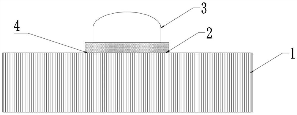
[0022] Such as figure 1 As shown, an organic light emitting diode frit glue packaging structure of the present invention includes a cover plate, a micro-nano thin layer and firt glue, the micro-nano thin layer is arranged on the cover plate, and the firt glue is arranged on the micro-nano thin layer ;The presence of micro-nano thin layer can improve the bonding surface between frit and cover plate, increase the contact angle between frit glue and cover plate before pre-sintering, so that the glue has fluidity while maintaining glue height; during sintering, frit-cover plate The interfacial bonding force between the glasses is strengthened, reducing the risk of water and oxygen intrusion and prolonging the life of OLED devices.

[0023] The cover plate is provided with a firt glue-filling channel; the micro-nano thin layer is arranged on the firt glue-filling channel by coating and chemical vapor deposition, and the micro-nano thin layer protrudes from the cover plate; A micro...

Embodiment 2

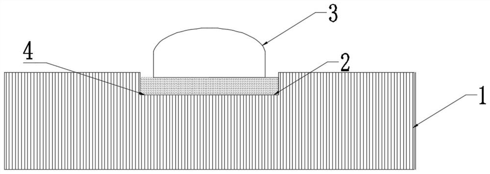
[0029] Such as figure 2 As shown, an organic light emitting diode frit glue packaging structure of the present invention includes a cover plate, a micro-nano thin layer and firt glue, the micro-nano thin layer is arranged on the cover plate, and the firt glue is arranged on the micro-nano thin layer ;The presence of micro-nano thin layer can improve the bonding surface between frit and cover plate, increase the contact angle between frit glue and cover plate before pre-sintering, so that the glue has fluidity while maintaining glue height; during sintering, frit-cover plate The interfacial bonding force between the glasses is strengthened, reducing the risk of water and oxygen intrusion and prolonging the life of OLED devices.

[0030] The cover plate is provided with a firt glue-filled channel, and the micro-nano thin layer is provided on the firt glue-filled channel through laser, corona, and etching. The micro-nano thin layer is embedded in the cover plate, and the micro-n...


PUM

PropertyMeasurementUnit
thicknessaaaaaaaaaa
thicknessaaaaaaaaaa

Abstract

The invention discloses an organic light-emitting diode frit glue packaging structure and a manufacturing method thereof. The organic light-emitting diode frit glue packaging structure comprises a cover plate, a micro-nano thin layer and frit glue, wherein the micro-nano thin layer is arranged on the cover plate, and the frit glue is arranged on the micro-nano thin layer. The invention belongs to the technical field of semiconductor packaging, and particularly relates to the organic light-emitting diode frit glue packaging structure and the manufacturing method thereof. A micro-nano thin layer is added on the surface of the cover plate, and the combination surface of the frit glue and the cover plate is improved.

Description

technical field [0001] The invention belongs to the technical field of semiconductor encapsulation, and specifically refers to an organic light emitting diode frit encapsulation structure and a manufacturing method thereof. Background technique [0002] Organic Light Emitting Diode (OLED) OLED display has the characteristics of low power consumption, wide viewing angle, wide color gamut, fast response speed, ultra-light and thin, etc. In the high-performance display area, it is developing more and more as an autonomous light-emitting device. faster; [0003] At present, the packaging methods used by OLED devices can be divided into two types, rigid and flexible. Among them, small rigid screens mainly adopt frit packaging, and frit packaging needs to rely on screen printing to print the glue on the glass cover, and then pre-sintering to remove The organic solvent in the colloid melts the glass powder in the colloid into pieces and sticks together with the cover glass, and fi...

Claims


Application Information

Patent Timeline
Patent Type & Authority Applications(China)
IPC IPC(8): H01L51/52H01L51/56
CPCH10K50/8426H10K71/00
Inventor 庄丹丹孙玉俊
Owner FUJIAN HUAJIACAI CO LTD
Learn More