Preparation method of heterojunction battery

A heterojunction cell and impurity technology, applied in circuits, photovoltaic power generation, electrical components, etc., can solve the problems of heterojunction cell photoelectric conversion efficiency distribution trailing, high cost, etc.

Pending Publication Date: 2021-11-19
宣城睿晖宣晟企业管理中心合伙企业(有限合伙)
View PDF0 Cites 1 Cited by
  • Summary
  • Abstract
  • Description
  • Claims
  • Application Information

AI Technical Summary

Problems solved by technology

[0004] The technical problem to be solved by the present invention is to overcome the problems of trailing photoelectric conversion efficiency distribution and high cost of heterojunction cells in the prior art

Method used


Image

  • Preparation method of heterojunction battery
  • Preparation method of heterojunction battery
  • Preparation method of heterojunction battery

Examples


Embodiment 1

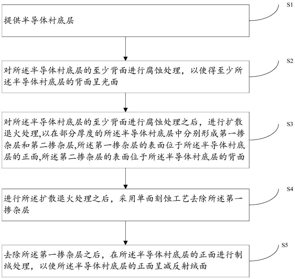
[0046] The embodiment of the present invention provides a preparation method of a heterojunction battery, please refer to figure 1 , including the following steps:

[0047] S1: providing a semiconductor substrate layer;

[0048] S2: performing etching treatment on at least the back side of the semiconductor substrate layer, so that at least the back side of the semiconductor substrate layer is a smooth surface;

[0049] S3: After performing etching treatment on at least the back side of the semiconductor substrate layer, perform diffusion annealing treatment to form a first doped layer and a second doped layer in a partial thickness of the semiconductor substrate layer, the first doped layer The surface of the doped layer is located on the front side of the semiconductor substrate layer, and the surface of the second doped layer is located on the back side of the semiconductor substrate layer;

[0050] S4: After performing the diffusion annealing treatment, remove the first ...

Embodiment 2

[0106] Another embodiment of the present invention also provides a method for preparing a heterojunction battery, which is combined below Figure 10 to Figure 11 Make a detailed introduction.

[0107] refer to Figure 10 , Figure 10 for Figure 7 Based on the schematic diagram, compared with Embodiment 1, this embodiment also removes the second doped layer 112 on the basis of removing the second oxide layer 132 .

[0108] In this embodiment, the second doped layer 112 is removed during the process of removing the second oxide layer 132 . Specifically, after the rounding process is performed, the second oxide layer 132 and the second doped layer 112 are removed.

[0109] The process of removing the second oxide layer 132 and the second doped layer 112 adopts a wet etching process. Specifically, the second oxide layer 132 and the second doped layer 112 are removed by chain cleaning. The method improves the efficiency of removing the second oxide layer 132 and the second do...


PUM

PropertyMeasurementUnit
thicknessaaaaaaaaaa
thicknessaaaaaaaaaa
thicknessaaaaaaaaaa

Abstract

A preparation method of a heterojunction battery comprises the following steps of providing a semiconductor substrate layer, carrying out corrosion treatment on at least the back surface of the semiconductor substrate layer so as to enable at least the back surface of the semiconductor substrate layer to be a smooth surface, after at least the back surface of the semiconductor substrate layer is subjected to corrosion treatment, conducting diffusion annealing treatment, so that a first doping layer and a second doping layer are respectively formed in the semiconductor substrate layer with partial thickness, the surface of the first doping layer is located on the front surface of the semiconductor substrate layer, and the surface of the second doping layer is positioned on the back surface of the semiconductor substrate layer, after the diffusion annealing treatment is carried out, adopting a single-side etching process to remove the first doping layer, and after the first doping layer is removed, conducting texturing processing on the front surface of the semiconductor substrate layer, so that the front surface of the semiconductor substrate layer is an antireflection textured surface. According to the method, the distribution trailing of the photoelectric conversion efficiency of the heterojunction cell is avoided, and the cost is reduced.

Description

technical field [0001] The invention relates to the field of semiconductors, in particular to a method for preparing a heterojunction battery. Background technique [0002] A solar cell is a device that directly converts solar radiation energy into electrical energy through the photoelectric effect by absorbing sunlight. Solar cells are a kind of clean energy cells, which are widely used in life and production. Heterojunction with intrinsic Thinlayer (HJT) cell is an important solar cell. The structure of the heterojunction cell is centered on the N-type silicon substrate, and P-type amorphous silicon and N-type silicon are formed on both sides of it. Type amorphous silicon, and then add a layer of intrinsic amorphous silicon film between the P-type amorphous silicon and N-type amorphous silicon and the N-type silicon substrate. After taking this process measure, the performance of the PN junction is improved, so The conversion efficiency of the heterojunction cell is impr...

Claims


Application Information

Patent Timeline
Patent Type & Authority Applications(China)
IPC IPC(8): H01L31/18H01L31/0236H01L31/0745
CPCH01L31/0745H01L31/02366H01L31/1804H01L31/1864Y02E10/50Y02E10/547Y02P70/50
Inventor 符欣周肃龚道仁王文静徐晓华姚真真程尚之
Owner 宣城睿晖宣晟企业管理中心合伙企业(有限合伙)
Why Eureka
Try Eureka