PCB winding device and power supply module
A power module, PCB board technology, applied in the direction of transformer/inductor cooling, transformer/inductor parts, transformer/inductor coil/winding/connection, etc., can solve the problem of wasting the available layers of PCB board, and achieve simplification Structure and process, solve heat accumulation, improve the effect of heat conduction efficiency
- Summary
- Abstract
- Description
- Claims
- Application Information
AI Technical Summary
Problems solved by technology
Method used
Image
Examples
Embodiment 1
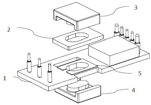
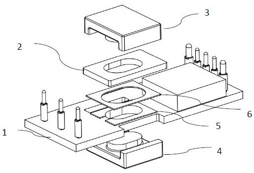
[0038] Such as Figure 4 As shown, the PCB transformer adopting the concept of the present invention includes: a main PCB multilayer board 1 and a secondary PCB multilayer board 2, a transformer magnetic core 3, and a transformer magnetic core 4, wherein the main PCB multilayer board 1 is used as the first A PCB board, and the sub-PCB multilayer board 2 serves as the second PCB board.
[0039] The main PCB multilayer board 1 and the auxiliary PCB multilayer board 2 are used to form a transformer winding, wherein the main PCB multilayer board 1 is used to form a part of the transformer winding, and the auxiliary PCB multilayer board 2 is used to form another part of the transformer winding. It should be noted that the windings formed on the main PCB multilayer board 1 and the windings formed on the auxiliary PCB multilayer board 2 do not need to be strictly differentiated according to the primary winding or the secondary winding. In some embodiments, the complete primary windi...
Embodiment 2
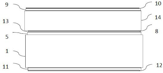
[0047] The difference between this embodiment and Embodiment 1 and Embodiment 2 is that since there is no need to consider the short circuit problem between the main PCB multilayer board and the secondary PCB multilayer board, in this embodiment, the first copper foil layer 5 and the second The solder resist layer provided on the surface of the copper foil layer 8 does not need to be removed. When the main PCB multilayer board 1 and the auxiliary PCB multilayer board 2 are assembled, the pads are still used to fix the main PCB multilayer board 1 and the auxiliary PCB multilayer board 2, and the solder resist layer on the first copper foil layer 5 and the second copper foil layer The solder resist layer on the foil layer 8 is arranged adjacently with a certain gap, or the solder resist layer on the first copper foil layer 5 and the solder resist layer on the second copper foil layer 8 are arranged in close contact. The gaps left by adjacent solder mask layers can be used as hea...
Embodiment 3
[0050] The concept of the present invention can also realize PCB inductance, and the specific implementation method is roughly the same as the aforementioned PCB transformer implementation, including the main PCB multilayer board and the auxiliary PCB multilayer board, but no magnetic core is required.
[0051] The main PCB multilayer board and the auxiliary PCB multilayer board are respectively used to form a part of the inductor winding, the main PCB multilayer board forms the first winding, the auxiliary PCB multilayer board forms the second winding, the main PCB multilayer board and the auxiliary PCB multilayer board After the boards are combined, the first winding and the second winding form a complete inductor. Wherein, the outermost copper foil layers on the side facing each other of the main PCB multilayer board and the auxiliary PCB multilayer board are used to form windings, and the electrical properties of the first winding and the second winding are the same.
[00...
PUM
 Abstract
Description
Claims
Application Information


