Device and method for growing silicon carbide crystals via liquid phase method

A technology of silicon carbide and liquid phase method, applied in chemical instruments and methods, single crystal growth, crystal growth, etc., can solve the problem of reducing the quality of growing crystals, sustainable crystal growth, increasing crystal growth costs, and reducing temperature gradients, etc. problem, to achieve long-term stable growth, increase output, and improve quality

Active Publication Date: 2021-11-30
北京晶格领域半导体有限公司
View PDF6 Cites 12 Cited by
  • Summary
  • Abstract
  • Description
  • Claims
  • Application Information

AI Technical Summary

Problems solved by technology

Further lead to the reduction of the proportion of silicon in the solution, the smaller distance between the growth end (at the solid-liquid interface) and the raw material end (the bottom of the graphite crucible), and the smaller temperature gradient, which will reduce the quality of the grown crystal and the sustainable progress of crystal growth.
At present, it is only possible to use a larger crucible and load more co-solution to offset the influence of the co-solution composition and temperature field during the growth process, but this will increase the cost of crystal growth.

Method used


Image

  • Device and method for growing silicon carbide crystals via liquid phase method
  • Device and method for growing silicon carbide crystals via liquid phase method
  • Device and method for growing silicon carbide crystals via liquid phase method

Examples


Embodiment 1

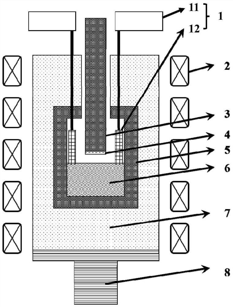
[0052] The Si alloy auxiliary solution used in this embodiment is composed of three phases of Si, Cr, and Al, and its atomic ratio is Si: 50%, Cr: 40%, and Al: 10%. Mix the elemental particles of the three raw materials evenly, place them in a graphite crucible, and figure 1 The structure shown is placed in a device for growing silicon carbide crystals by the liquid phase method, and the air in the crucible is evacuated to 2×10 by a molecular pump. -4 After the Pa is lower than 1.5 atm Ar gas is introduced as a protective gas and the crucible is heated. When the temperature in the crucible reaches the melting temperature of the growth raw material, Si, Cr and Al in the graphite crucible are all melted to obtain a Si alloy auxiliary solution. In the embodiment, the initial position of the liquid level maintaining ring of the liquid level maintaining device should be adjusted to a position where its lower end is 1-3mm lower than the Si alloy solution level when the furnace is in...

Embodiment 2

[0056] Embodiment 2 is basically the same as Embodiment 1, the difference is:

[0057] During the growth of silicon carbide crystals, the silicon carbide seed crystal is slowly pulled at a speed of 0.2 mm / h, and the liquid level maintaining ring of the liquid level maintaining device is lowered into the Si alloy auxiliary solution at a speed of 0.2 mm / h.

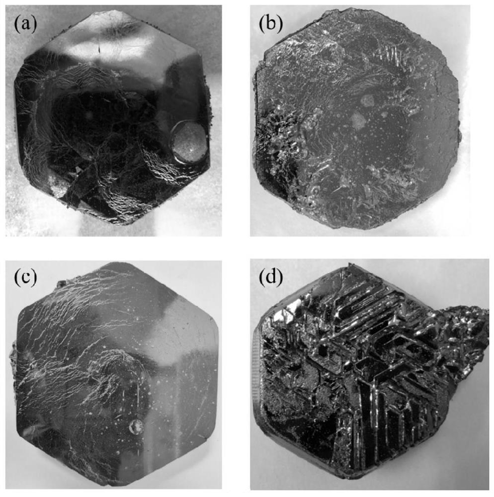
[0058] The appearance figure (top view) of the silicon carbide crystal that present embodiment grows obtains, as figure 2 as shown in (b); from figure 2 (b) It can be seen that the surface of the silicon carbide crystal in this example has many undulations and ravines, which are mixed with Si alloy co-solution and silicon carbide polycrystalline particles, and the quality of the silicon carbide crystal deteriorates.

[0059] Diameter change diagram of the silicon carbide crystal grown in the present embodiment, such as Figure 4 shown; from Figure 4 It can be seen that during the whole growth process, the diameter of s...

Embodiment 3

[0061] Embodiment 3 is basically the same as Embodiment 1, the difference is:

[0062] After the entire growth process lasted for 90 hours, the silicon carbide seed crystal was pulled up at a speed of 3 mm / h to separate the grown silicon carbide crystal from the liquid surface of the Si alloy co-solution, and slowly cooled to room temperature, that is, the entire liquid-phase method of silicon carbide The crystal growth process is completed, and silicon carbide crystals are obtained.

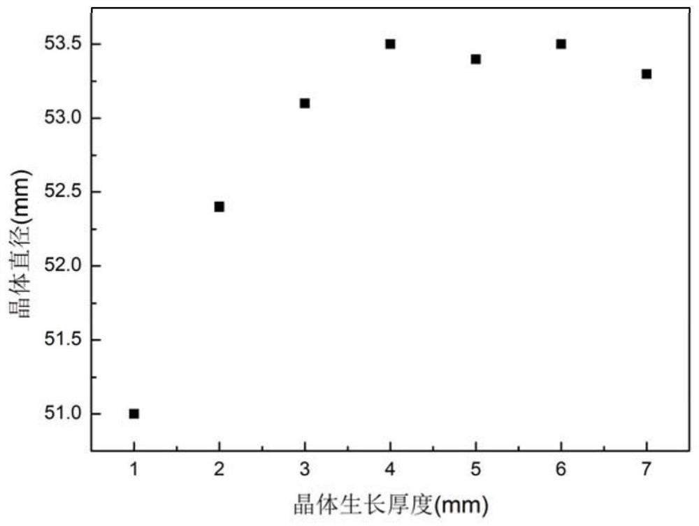
[0063] In this embodiment, the growth crystal diameter varies with the growth thickness as Figure 5 As shown, the outline view (top view) of the surface of the silicon carbide crystal grown in this embodiment is as figure 2 Shown in (c); As can be seen from the growth results, the growth thickness of the silicon carbide crystal grown in this embodiment reaches 10.5mm, and the surface of the silicon carbide growth crystal is neat and clean, and the diameter of the silicon carbide growth crysta...


PUM

PropertyMeasurementUnit
thicknessaaaaaaaaaa
thicknessaaaaaaaaaa
densityaaaaaaaaaa

Abstract

The invention relates to a device and a method for growing silicon carbide crystals via a liquid phase method. The device comprises a crucible for accommodating a Si alloy assistant solution and a seed crystal rod for fixing a silicon carbide seed crystal; and the device further comprises a liquid level height keeping device, wherein the liquid level height keeping device comprises a circular liquid level keeping ring and a pushing device used for pushing the circular liquid level keeping ring to descend into the Si alloy assistant solution. The method comprises the following steps: melting a growth raw material containing Si and a metal simple substance into the Si alloy assistant solution; and lowering the silicon carbide seed crystal for contacting with the assistant solution to grow the silicon carbide crystals, wherein in the growth process of the silicon carbide crystals, the circular liquid level maintaining ring is pushed by the pushing device to descend into the Si alloy assistant solution so as to keep the liquid level height of the Si alloy assistant solution unchanged. According to the invention, the liquid level in the growth process of the silicon carbide crystals is not changed, a temperature field is kept constant, the stability of the assistant solution components can be kept, and the thickness of the generated silicon carbide crystals is improved.

Description

technical field [0001] The invention belongs to the technical field of liquid-phase production of silicon carbide single crystals, and in particular relates to a device and method for growing silicon carbide crystals by a liquid-phase method. Background technique [0002] Silicon carbide is one of the wide-bandgap semiconductor materials that has received widespread attention. It has the advantages of low density, large band gap, high breakdown field strength, high saturated electron mobility, good thermal stability and chemical stability, etc. , high voltage, high power devices and ideal substrate materials for blue light emitting diodes. [0003] The current main growth method of silicon carbide is the physical vapor transport method. Although this method is relatively mature and has supplied a large number of silicon carbide single crystal substrates to the market, due to the poor stability of the gas growth environment during the gas phase growth process, its growth in t...

Claims


Application Information

Patent Timeline
Patent Type & Authority Applications(China)
IPC IPC(8): C30B29/36C30B9/10
CPCC30B29/36C30B9/10
Inventor 张泽盛
Owner 北京晶格领域半导体有限公司
Why Eureka
Try Eureka